- 您现在的位置:买卖IC网 > PDF目录19665 > XC2C512-7PQG208C (Xilinx Inc)IC CR-II CPLD 512MCELL 208PQFP PDF资料下载
参数资料
| 型号: | XC2C512-7PQG208C |
| 厂商: | Xilinx Inc |
| 文件页数: | 4/16页 |
| 文件大小: | 0K |
| 描述: | IC CR-II CPLD 512MCELL 208PQFP |
| 标准包装: | 24 |
| 系列: | CoolRunner II |
| 可编程类型: | 系统内可编程 |
| 最大延迟时间 tpd(1): | 7.1ns |
| 电压电源 - 内部: | 1.7 V ~ 1.9 V |
| 逻辑元件/逻辑块数目: | 32 |
| 宏单元数: | 512 |
| 门数: | 12000 |
| 输入/输出数: | 173 |
| 工作温度: | 0°C ~ 70°C |
| 安装类型: | 表面贴装 |
| 封装/外壳: | 208-BFQFP |
| 供应商设备封装: | 208-PQFP(28x28) |
| 包装: | 托盘 |
CoolRunner-II CPLD Family
12
DS090 (v3.1) September 11, 2008
Product Specification
R
Programming
The programming data sequence is delivered to the device
using either Xilinx iMPACT software and a Xilinx download
cable,
a
third-party
JTAG
development
system,
a
JTAG-compatible board tester, or a simple microprocessor
interface that emulates the JTAG instruction sequence. The
iMPACT software also outputs serial vector format (SVF)
files for use with any tools that accept SVF format, including
automatic test equipment. See CoolRunner-II CPLD
Application Notes for more information on how to program.
In System Programming
All CoolRunner-II CPLD parts are 1.8V in system program-
mable. This means they derive their programming voltage
and currents from the 1.8V VCC (internal supply voltage)
pins on the part. The VCCIO pins do not participate in this
operation, as they might assume another voltage ranging as
high as 3.3V down to 1.5V (however, all VCCIO, VCCINT,
VCCAUX, and GND pins must be connected for the device to
be programmed, and operate correctly). A 1.8V VCC is
required to properly operate the internal state machines and
charge pumps that reside within the CPLD to do the nonvol-
atile programming operations. I/O pins are not in user mode
during JTAG programming; they are held in 3-state with a
weak pullup. The JTAG interface buffers are powered by a
dedicated power pin, VCCAUX, which is independent of all
other supply pins. VCCAUX must be connected. Xilinx soft-
ware is provided to deliver the bitstream to the CPLD and
drive the appropriate IEEE 1532 protocol. To that end, there
is a set of IEEE 1532 commands that are supported in the
CoolRunner-II CPLD parts. Programming times are less
than one second for 32 to 256 macrocell parts. Program-
ming times are less than four seconds for 384 and 512 mac-
rocell parts. Programming of CoolRunner-II CPLDs is only
guaranteed when operating in the commercial temperature
and voltage ranges as defined in the device-specific data
sheets.
On-The-Fly Reconfiguration (OTF)
The Xilinx ISE 5.2i tool supports OTF for CoolRunner-II
CPLDs. This permits programming a new nonvolatile pat-
tern into the part while another pattern is currently in use.
OTF has the same voltage and temperature specifications
as system programming. During pattern transition I/O pins
are in high impedance with a weak pullup to VCCIO. Transi-
tion time typically lasts between 50 and 300
μs, depending
on density. See XAPP388 for more information.
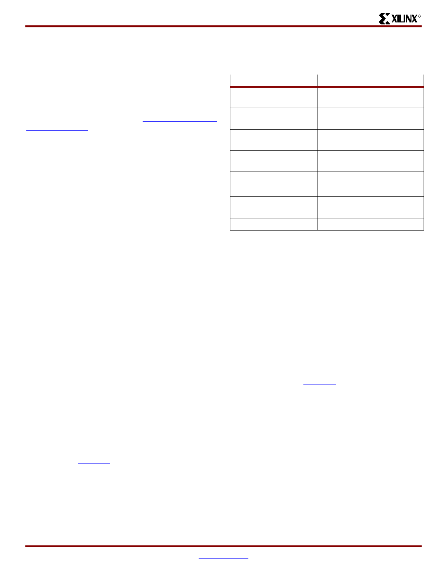
JTAG Instructions
Table 7 shows the commands available to users. These
same commands can be used by third party ATE products,
as well. The internal controllers can operate as fast as
66 MHz.
Power-Up Characteristics
CoolRunner-II CPLD parts must operate under the
demands of both the high-speed and the portable market
places; therefore, they must support hot plugging for the
high-speed world and tolerate most any power sequence to
its various voltage pins. They must also not draw excessive
current during power-up initialization. To those ends, the
general behavior is summarized as follows:
1.
I/O pins are disabled until the end of power-up.
2.
As supply rises, configuration bits transfer from
nonvolatile memory to SRAM cells.
3.
As power up completes, the outputs become as
configured (input, output, or I/O).
4.
For specific configuration times and power up
requirements, see XAPP389.
CoolRunner-II CPLD I/O pins are well behaved under all
operating conditions. During power-up, CoolRunner-II
devices employ internal circuitry which keeps the devices in
the quiescent state until the VCCINT supply voltage is at a
safe level (approximately 1.3V). In the quiescent state,
JTAG pins are disabled, and all device outputs are disabled
with the pins weakly pulled High, as shown in Table 8. When
the supply voltage reaches a safe level, all user registers
become initialized, and the device is immediately available
for operation, as shown in Figure 12. Best results are
obtained with a smooth VCC rise in less than 4 ms. Final
VCC value should occur within 1 second.
If the device is in the erased state (before any user pattern
is programmed), the device outputs remain disabled with a
weak pull-up. The JTAG pins are enabled to allow the device
Table 7: JTAG Instructions
Code
Instruction
Description
00000000
EXTEST
Force boundary scan data onto
outputs
00000011
PRELOAD
Latch macrocell data into
boundary scan cells
11111111
BYPASS
Insert bypass register between
TDI and TDO
00000010
INTEST
Force boundary scan data onto
inputs and feedbacks
00000001
IDCODE
Read IDCODE
11111101
USERCODE Read USERCODE
11111100
HIGHZ
Force output into high
impedance state
11111010
CLAMP
Latch present output state
相关PDF资料 |
PDF描述 |
|---|---|
| DS1624+ | IC THERM/EEPROM DIG 256BYTE 8DIP |
| GCC08DCSN | CONN EDGECARD 16POS DIP .100 SLD |
| PQ1R30 | IC REG LDO 3V .15A SOT-23L |
| XCR3384XL-12PQ208C | IC CPLD 3.3V ZERO PWR 208-PQFP |
| GCC08DCSH | CONN EDGECARD 16POS DIP .100 SLD |
相关代理商/技术参数 |
参数描述 |
|---|---|
| XC2C64 | 制造商:XILINX 制造商全称:XILINX 功能描述:This lends power savings to High-end Communication equipment and speed to battery operated devices. |
| XC2C64-4CP56C | 制造商:XILINX 制造商全称:XILINX 功能描述:This lends power savings to High-end Communication equipment and speed to battery operated devices. |
| XC2C64-4PC44C | 制造商:XILINX 制造商全称:XILINX 功能描述:This lends power savings to High-end Communication equipment and speed to battery operated devices. |
| XC2C64-4VQ100C | 制造商:XILINX 制造商全称:XILINX 功能描述:This lends power savings to High-end Communication equipment and speed to battery operated devices. |
| XC2C64-4VQ44C | 制造商:XILINX 制造商全称:XILINX 功能描述:This lends power savings to High-end Communication equipment and speed to battery operated devices. |
发布紧急采购,3分钟左右您将得到回复。