参数资料
| 型号: | XC2S100-6TQ144C |
| 厂商: | Xilinx Inc |
| 文件页数: | 35/99页 |
| 文件大小: | 0K |
| 描述: | IC FPGA 2.5V C-TEMP 144-TQFP |
| 标准包装: | 60 |
| 系列: | Spartan®-II |
| LAB/CLB数: | 600 |
| 逻辑元件/单元数: | 2700 |
| RAM 位总计: | 40960 |
| 输入/输出数: | 92 |
| 门数: | 100000 |
| 电源电压: | 2.375 V ~ 2.625 V |
| 安装类型: | 表面贴装 |
| 工作温度: | 0°C ~ 85°C |
| 封装/外壳: | 144-LQFP |
| 供应商设备封装: | 144-TQFP(20x20) |
第1页第2页第3页第4页第5页第6页第7页第8页第9页第10页第11页第12页第13页第14页第15页第16页第17页第18页第19页第20页第21页第22页第23页第24页第25页第26页第27页第28页第29页第30页第31页第32页第33页第34页当前第35页第36页第37页第38页第39页第40页第41页第42页第43页第44页第45页第46页第47页第48页第49页第50页第51页第52页第53页第54页第55页第56页第57页第58页第59页第60页第61页第62页第63页第64页第65页第66页第67页第68页第69页第70页第71页第72页第73页第74页第75页第76页第77页第78页第79页第80页第81页第82页第83页第84页第85页第86页第87页第88页第89页第90页第91页第92页第93页第94页第95页第96页第97页第98页第99页
Spartan-II FPGA Family: Functional Description
DS001-2 (v2.8) June 13, 2008
Module 2 of 4
Product Specification
40
R
LVTTL output buffers have selectable drive strengths.
The format for LVTTL OBUF primitive names is as follows.
OBUF_<slew_rate>_<drive_strength>
<slew_rate> is either F (Fast), or S (Slow) and
<drive_strength> is specified in milliamps (2, 4, 6, 8, 12, 16,
or 24). The default is slew rate limited with 12 mA drive.
OBUF placement restrictions require that within a given
VCCO bank each OBUF share the same output source drive
voltage. Input buffers of any type and output buffers that do
not require VCCO can be placed within any VCCO bank.
Table 17 summarizes the output compatibility requirements.
The LOC property can specify a location for the OBUF.
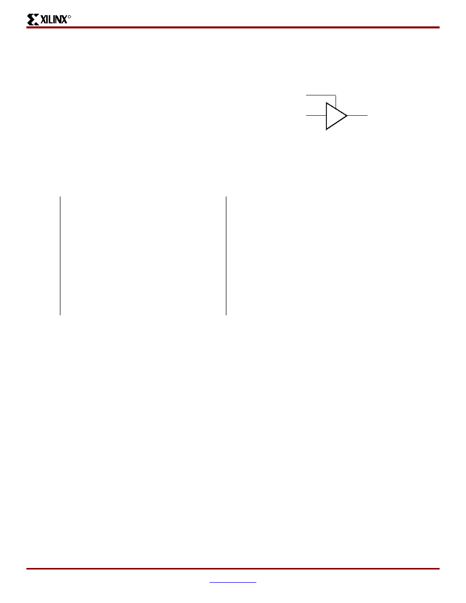
OBUFT
The generic 3-state output buffer OBUFT, shown in
Figure 39, typically implements 3-state outputs or
bidirectional I/O.
With no extension or property specified for the generic
OBUFT primitive, the assumed standard is slew rate limited
LVTTL with 12 mA drive strength.
The LVTTL OBUFT can support one of two slew rate modes
to minimize bus transients. By default, the slew rate for each
output buffer is reduced to minimize power bus transients
when switching non-critical signals.
LVTTL 3-state output buffers have selectable drive
strengths.
The format for LVTTL OBUFT primitive names is as follows.
OBUFT_<slew_rate>_<drive_strength>
<slew_rate> can be either F (Fast), or S (Slow) and
<drive_strength> is specified in milliamps (2, 4, 6, 8, 12, 16,
or 24).
The Versatile I/O OBUFT placement restrictions require
that within a given VCCO bank each OBUFT share the same
output source drive voltage. Input buffers of any type and
output buffers that do not require VCCO can be placed within
the same VCCO bank.
The LOC property can specify a location for the OBUFT.
3-state output buffers and bidirectional buffers can have
either a weak pull-up resistor, a weak pull-down resistor, or
a weak "keeper" circuit. Control this feature by adding the
appropriate primitive to the output net of the OBUFT
(PULLUP, PULLDOWN, or KEEPER).
The weak "keeper" circuit requires the input buffer within the
IOB to sample the I/O signal. So, OBUFTs programmed for
an I/O standard that requires a VREF have automatic
placement of a VREF in the bank with an OBUFT configured
with a weak "keeper" circuit. This restriction does not affect
most circuit design as applications using an OBUFT
configured with a weak "keeper" typically implement a
bidirectional I/O. In this case the IBUF (and the
corresponding VREF) are explicitly placed.
The LOC property can specify a location for the OBUFT.
IOBUF
Use the IOBUF primitive for bidirectional signals that
require both an input buffer and a 3-state output buffer with
an active high 3-state pin. The generic input/output buffer
IOBUF appears in Figure 40.
With no extension or property specified for the generic
IOBUF primitive, the assumed standard is LVTTL input
buffer and slew rate limited LVTTL with 12 mA drive strength
for the output buffer.
The LVTTL IOBUF can support one of two slew rate modes
to minimize bus transients. By default, the slew rate for each
output buffer is reduced to minimize power bus transients
when switching non-critical signals.
LVTTL bidirectional buffers have selectable output drive
strengths.
The format for LVTTL IOBUF primitive names is as follows:
Table 17: Output Standards Compatibility
Requirements
Rule 1
Only outputs with standards which share
compatible VCCO may be used within the same
bank.
Rule 2
There are no placement restrictions for outputs
with standards that do not require a VCCO.
VCCO
Compatible Standards
3.3
LVTTL, SSTL3_I, SSTL3_II, CTT, AGP, GTL,
GTL+, PCI33_3, PCI66_3
2.5
SSTL2_I, SSTL2_II, LVCMOS2, GTL, GTL+
1.5
HSTL_I, HSTL_III, HSTL_IV, GTL, GTL+
Figure 39: 3-State Output Buffer Primitive (OBUFT
IO
I
IOBUFT
DS001_39_032300
T
相关PDF资料 |
PDF描述 |
|---|---|
| XC2S100-5TQ144I | IC FPGA 2.5V I-TEMP 144-TQFP |
| 24LC64FT-I/SN | IC SRL EEPROM 8KX8 2.5V 8-SOIC |
| XC3S400A-4FT256I | IC SPARTAN-3A FPGA 400K 256FTBGA |
| XC3S200AN-4FT256I | IC FPGA SPARTAN 3AN 256FTBGA |
| XC3S400AN-4FTG256C | IC FPGA SPARTAN-3AN 256FTBGA |
相关代理商/技术参数 |
参数描述 |
|---|---|
| XC2S100-6TQ144I | 制造商:XILINX 制造商全称:XILINX 功能描述:Spartan-II 2.5V FPGA Family:Introduction and Ordering Information |
| XC2S100-6TQG144C | 制造商:Xilinx 功能描述:FPGA SPARTAN-II 100K GATES 2700 CELLS 263MHZ 2.5V 144TQFP EP - Trays |
| XC2S100-6TQG144I | 制造商:XILINX 制造商全称:XILINX 功能描述:Spartan-II FPGA Family |
| XC2S100-6VQ100C | 制造商:XILINX 制造商全称:XILINX 功能描述:Spartan-II FPGA Family |
| XC2S100-6VQ100I | 制造商:XILINX 制造商全称:XILINX 功能描述:Spartan-II 2.5V FPGA Family:Introduction and Ordering Information |
发布紧急采购,3分钟左右您将得到回复。