参数资料
| 型号: | XC2S100-6TQ144C |
| 厂商: | Xilinx Inc |
| 文件页数: | 68/99页 |
| 文件大小: | 0K |
| 描述: | IC FPGA 2.5V C-TEMP 144-TQFP |
| 标准包装: | 60 |
| 系列: | Spartan®-II |
| LAB/CLB数: | 600 |
| 逻辑元件/单元数: | 2700 |
| RAM 位总计: | 40960 |
| 输入/输出数: | 92 |
| 门数: | 100000 |
| 电源电压: | 2.375 V ~ 2.625 V |
| 安装类型: | 表面贴装 |
| 工作温度: | 0°C ~ 85°C |
| 封装/外壳: | 144-LQFP |
| 供应商设备封装: | 144-TQFP(20x20) |
第1页第2页第3页第4页第5页第6页第7页第8页第9页第10页第11页第12页第13页第14页第15页第16页第17页第18页第19页第20页第21页第22页第23页第24页第25页第26页第27页第28页第29页第30页第31页第32页第33页第34页第35页第36页第37页第38页第39页第40页第41页第42页第43页第44页第45页第46页第47页第48页第49页第50页第51页第52页第53页第54页第55页第56页第57页第58页第59页第60页第61页第62页第63页第64页第65页第66页第67页当前第68页第69页第70页第71页第72页第73页第74页第75页第76页第77页第78页第79页第80页第81页第82页第83页第84页第85页第86页第87页第88页第89页第90页第91页第92页第93页第94页第95页第96页第97页第98页第99页
Spartan-II FPGA Family: Pinout Tables
DS001-4 (v2.8) June 13, 2008
Module 4 of 4
Product Specification
70
R
Note: Some early versions of Spartan-II devices, including
the XC2S15 and XC2S30 ES devices and the XC2S150
with date code 0045 or earlier, included a power-down pin.
For more information, see Answer Record 10500.
VCCO Banks
Some of the I/O standards require specific VCCO voltages.
These voltages are externally connected to device pins that
serve groups of IOBs, called banks. Eight I/O banks result
from separating each edge of the FPGA into two banks (see
which must be connected to the same voltage. In the
smaller packages, the VCCO pins are connected between
banks, effectively reducing the number of independent
banks available (see Table 37). These interconnected
banks are shown in the Pinout Tables with VCCO pads for
multiple banks connected to the same pin.
Package Overview
Table 36 shows the six low-cost, space-saving production
package styles for the Spartan-II family.
Each package style is available in an environmentally
friendly lead-free (Pb-free) option. The Pb-free packages
include an extra ‘G’ in the package style name. For
example, the standard “CS144” package becomes
“CSG144” when ordered as the Pb-free option. Leaded
(non-Pb-free) packages may be available for selected
devices, with the same pin-out and without the "G" in the
ordering code; contact Xilinx sales for more information.
The mechanical dimensions of the standard and Pb-free
packages are similar, as shown in the mechanical drawings
provided in Table 38.
For additional package information, see UG112: Device
Package User Guide.
Mechanical Drawings
Detailed mechanical drawings for each package type are
available from the Xilinx web site at the specified location in
Table 38.
Material Declaration Data Sheets (MDDS) are also
available on the Xilinx web site for each package.
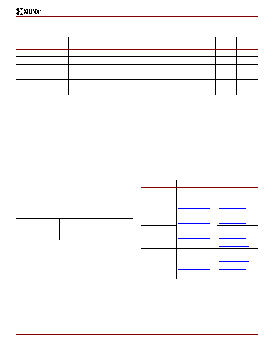
Table 36: Spartan-II Family Package Options
Package
Leads
Type
Maximum
I/O
Lead Pitch
(mm)
Footprint
Area (mm)
Height
(mm)
Mass(1)
(g)
VQ100 / VQG100
100
Very Thin Quad Flat Pack (VQFP)
60
0.5
16 x 16
1.20
0.6
TQ144 / TQG144
144
Thin Quad Flat Pack (TQFP)
92
0.5
22 x 22
1.60
1.4
CS144 / CSG144
144
Chip Scale Ball Grid Array (CSBGA)
92
0.8
12 x 12
1.20
0.3
PQ208 / PQG208
208
Plastic Quad Flat Pack (PQFP)
140
0.5
30.6 x 30.6
3.70
5.3
FG256 / FGG256
256
Fine-pitch Ball Grid Array (FBGA)
176
1.0
17 x 17
2.00
0.9
FG456 / FGG456
456
Fine-pitch Ball Grid Array (FBGA)
284
1.0
23 x 23
2.60
2.2
Notes:
1.
Package mass is
±10%.
Table 37: Independent VCCO Banks Available
Package
VQ100
PQ208
CS144
TQ144
FG256
FG456
Independent Banks
1
4
8
Table 38: Xilinx Package Documentation
Package
Drawing
MDDS
VQ100
VQG100
TQ144
TQG144
CS144
CSG144
PQ208
PQG208
FG256
FGG256
FG456
FGG456
相关PDF资料 |
PDF描述 |
|---|---|
| XC2S100-5TQ144I | IC FPGA 2.5V I-TEMP 144-TQFP |
| 24LC64FT-I/SN | IC SRL EEPROM 8KX8 2.5V 8-SOIC |
| XC3S400A-4FT256I | IC SPARTAN-3A FPGA 400K 256FTBGA |
| XC3S200AN-4FT256I | IC FPGA SPARTAN 3AN 256FTBGA |
| XC3S400AN-4FTG256C | IC FPGA SPARTAN-3AN 256FTBGA |
相关代理商/技术参数 |
参数描述 |
|---|---|
| XC2S100-6TQ144I | 制造商:XILINX 制造商全称:XILINX 功能描述:Spartan-II 2.5V FPGA Family:Introduction and Ordering Information |
| XC2S100-6TQG144C | 制造商:Xilinx 功能描述:FPGA SPARTAN-II 100K GATES 2700 CELLS 263MHZ 2.5V 144TQFP EP - Trays |
| XC2S100-6TQG144I | 制造商:XILINX 制造商全称:XILINX 功能描述:Spartan-II FPGA Family |
| XC2S100-6VQ100C | 制造商:XILINX 制造商全称:XILINX 功能描述:Spartan-II FPGA Family |
| XC2S100-6VQ100I | 制造商:XILINX 制造商全称:XILINX 功能描述:Spartan-II 2.5V FPGA Family:Introduction and Ordering Information |
发布紧急采购,3分钟左右您将得到回复。