参数资料
| 型号: | XC2S100E-6TQ144C |
| 厂商: | Xilinx Inc |
| 文件页数: | 12/108页 |
| 文件大小: | 0K |
| 描述: | IC FPGA 1.8V 600 CLB'S 144-TQFP |
| 产品变化通告: | FPGA Family Discontinuation 18/Apr/2011 |
| 标准包装: | 60 |
| 系列: | Spartan®-IIE |
| LAB/CLB数: | 600 |
| 逻辑元件/单元数: | 2700 |
| RAM 位总计: | 40960 |
| 输入/输出数: | 102 |
| 门数: | 100000 |
| 电源电压: | 1.71 V ~ 1.89 V |
| 安装类型: | 表面贴装 |
| 工作温度: | 0°C ~ 85°C |
| 封装/外壳: | 144-LQFP |
| 供应商设备封装: | 144-TQFP(20x20) |
| 其它名称: | 122-1206 |
第1页第2页第3页第4页第5页第6页第7页第8页第9页第10页第11页当前第12页第13页第14页第15页第16页第17页第18页第19页第20页第21页第22页第23页第24页第25页第26页第27页第28页第29页第30页第31页第32页第33页第34页第35页第36页第37页第38页第39页第40页第41页第42页第43页第44页第45页第46页第47页第48页第49页第50页第51页第52页第53页第54页第55页第56页第57页第58页第59页第60页第61页第62页第63页第64页第65页第66页第67页第68页第69页第70页第71页第72页第73页第74页第75页第76页第77页第78页第79页第80页第81页第82页第83页第84页第85页第86页第87页第88页第89页第90页第91页第92页第93页第94页第95页第96页第97页第98页第99页第100页第101页第102页第103页第104页第105页第106页第107页第108页
DS077-2 (v3.0) August 9, 2013
11
Product Specification
Spartan-IIE FPGA Family: Functional Description
R
— OBSOLETE — OBSOLETE — OBSOLETE — OBSOLETE —
Optional pull-up and pull-down resistors and an optional
weak-keeper circuit are attached to each user I/O pad. Prior
to configuration all outputs not involved in configuration are
forced into their high-impedance state. The pull-down resis-
tors and the weak-keeper circuits are inactive, but inputs
may optionally be pulled up. The activation of pull-up resis-
tors prior to configuration is controlled on a global basis by
the configuration mode pins. If the pull-up resistors are not
activated, all the pins will float. Consequently, external
pull-up or pull-down resistors must be provided on pins
required to be at a well-defined logic level prior to configura-
tion.
All pads are protected against damage from electrostatic
discharge (ESD) and from over-voltage transients. After
configuration, clamping diodes are connected to VCCO for
LVTTL, PCI, HSTL, SSTL, CTT, and AGP standards.
All Spartan-IIE FPGA IOBs support IEEE 1149.1-compati-
ble boundary scan testing.
Input Path
A buffer in the IOB input path routes the input signal directly
to internal logic and through an optional input flip-flop.
An optional delay element at the D-input of this flip-flop elim-
inates pad-to-pad hold time. The delay is matched to the
internal clock-distribution delay of the FPGA, and when
used, assures that the pad-to-pad hold time is zero.
Each input buffer can be configured to conform to any of the
low-voltage signaling standards supported. In some of
these standards the input buffer utilizes a user-supplied
threshold voltage, VREF. The need to supply VREF imposes
constraints on which standards can used in close proximity
to each other. See I/O Banking.
There are optional pull-up and pull-down resistors at each
input for use after configuration.
Output Path
The output path includes a 3-state output buffer that drives
the output signal onto the pad. The output signal can be
routed to the buffer directly from the internal logic or through
an optional IOB output flip-flop.
The 3-state control of the output can also be routed directly
from the internal logic or through a flip-flip that provides syn-
chronous enable and disable.
Each output driver can be individually programmed for a
wide range of low-voltage signaling standards. Each output
buffer can source up to 24 mA and sink up to 48 mA. Drive
strength and slew rate controls minimize bus transients. The
default output driver is LVTTL with 12 mA drive strength and
slow slew rate.
In most signaling standards, the output high voltage
depends on an externally supplied VCCO voltage. The need
to supply VCCO imposes constraints on which standards
can be used in close proximity to each other. See I/O Bank-
ing.
An optional weak-keeper circuit is connected to each out-
put. When selected, the circuit monitors the voltage on the
pad and weakly drives the pin High or Low to match the
input signal. If the pin is connected to a multiple-source sig-
nal, the weak keeper holds the signal in its last state if all
drivers are disabled. Maintaining a valid logic level in this
way helps eliminate bus chatter.
Because the weak-keeper circuit uses the IOB input buffer
to monitor the input level, an appropriate VREF voltage must
be provided if the signaling standard requires one. The pro-
vision of this voltage must comply with the I/O banking
rules.
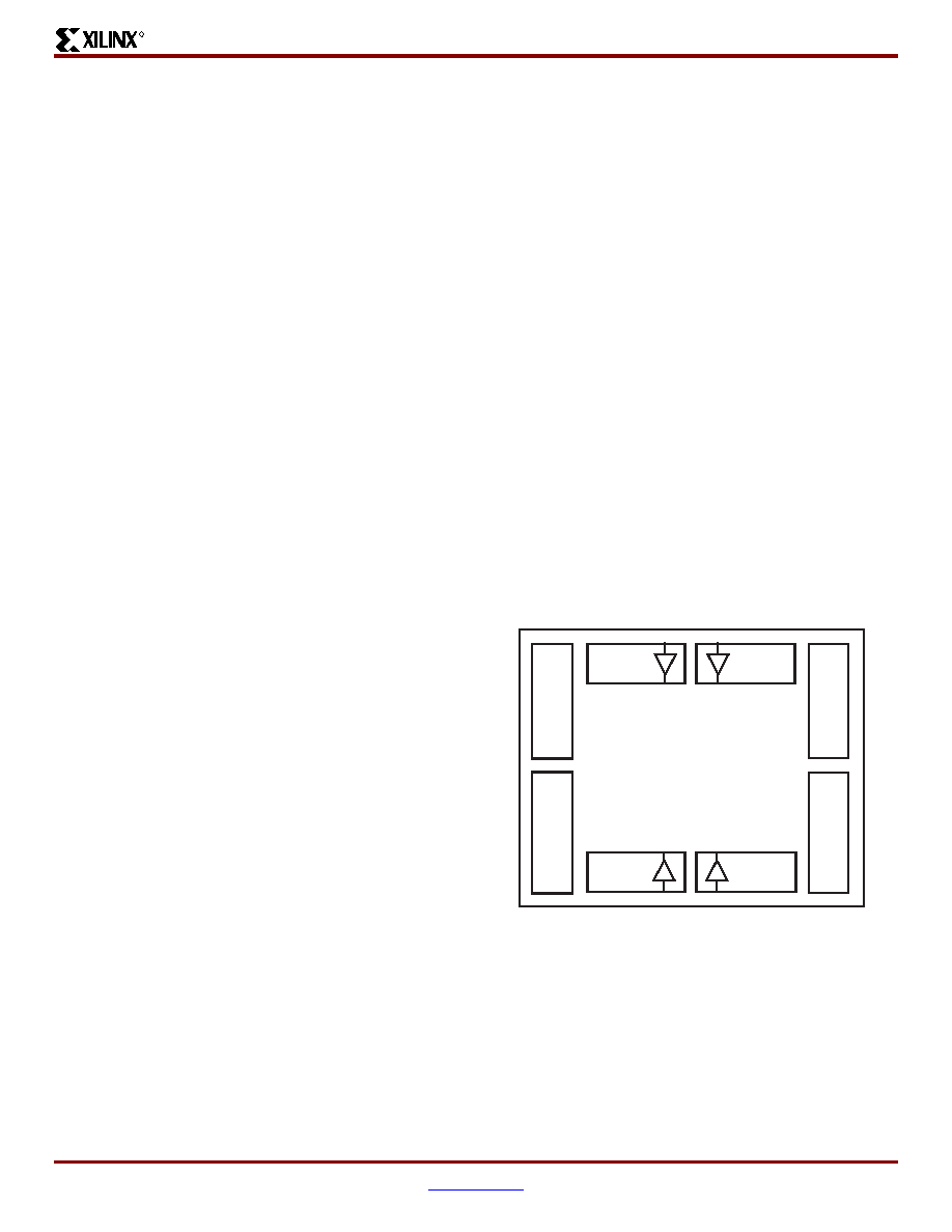
I/O Banking
Some of the I/O standards described above require VCCO
and/or VREF voltages. These voltages are externally sup-
plied and connected to device pins that serve groups of
IOBs, called banks. Consequently, restrictions exist about
which I/O standards can be combined within a given bank.
Eight I/O banks result from separating each edge of the
FPGA into two banks (see Figure 5). The pinout tables
show the bank affiliation of each I/O (see Pinout Tables,
connected to the same voltage. Voltage requirements are
determined by the output standards in use.
In the TQ144 and PQ208 packages, the eight banks have
VCCO connected together. Thus, only one VCCO level is
allowed in these packages, although different VREF values
are allowed in each of the eight banks.
Within a bank, standards may be mixed only if they use the
GTL and GTL+ appear under all voltages because their
open-drain outputs do not depend on VCCO. Note that VCCO
Figure 5: Spartan-IIE I/O Banks
DS077-2_02_051501
Bank 0
GCLK3
GCLK2
GCLK1
GCLK0
Bank 1
Bank 5
Bank 4
Spartan-IIE
Device
Bank
7
Bank
6
Bank
2
Bank
3
相关PDF资料 |
PDF描述 |
|---|---|
| XA3S200-4PQG208I | IC FPGA SPARTAN-3 200K 208-PQFP |
| 24FC64FT-I/SN | IC EEPROM 64KBIT 1MHZ 8SOIC |
| XA2S50E-6TQ144Q | IC FPGA SPARTAN-IIE 144TQFP |
| RSA50DTBD-S664 | CONN EDGECARD 100PS R/A .125 SLD |
| XC3S200-4PQ208I | IC FPGA SPARTAN 3 208PQFP |
相关代理商/技术参数 |
参数描述 |
|---|---|
| XC2S100E-6TQ144C0776 | 制造商:Xilinx 功能描述: |
| XC2S100E-6TQ144I | 制造商:XILINX 制造商全称:XILINX 功能描述:Spartan-IIE 1.8V FPGA Family |
| XC2S100E-6TQG144C | 功能描述:IC FPGA 1.8V 600 CLB'S 144-TQFP RoHS:是 类别:集成电路 (IC) >> 嵌入式 - FPGA(现场可编程门阵列) 系列:Spartan®-IIE 标准包装:40 系列:Spartan® 6 LX LAB/CLB数:3411 逻辑元件/单元数:43661 RAM 位总计:2138112 输入/输出数:358 门数:- 电源电压:1.14 V ~ 1.26 V 安装类型:表面贴装 工作温度:-40°C ~ 100°C 封装/外壳:676-BGA 供应商设备封装:676-FBGA(27x27) |
| XC2S100E-6TQG144I | 制造商:XILINX 制造商全称:XILINX 功能描述:Spartan-IIE FPGA |
| XC2S100E7FG456C | 制造商:Xilinx 功能描述: |
发布紧急采购,3分钟左右您将得到回复。