参数资料
| 型号: | XC2S15-5CS144C |
| 厂商: | Xilinx Inc |
| 文件页数: | 48/99页 |
| 文件大小: | 0K |
| 描述: | IC FPGA 2.5V C-TEMP 144-CSBGA |
| 标准包装: | 198 |
| 系列: | Spartan®-II |
| LAB/CLB数: | 96 |
| 逻辑元件/单元数: | 432 |
| RAM 位总计: | 16384 |
| 输入/输出数: | 86 |
| 门数: | 15000 |
| 电源电压: | 2.375 V ~ 2.625 V |
| 安装类型: | 表面贴装 |
| 工作温度: | 0°C ~ 85°C |
| 封装/外壳: | 144-TFBGA,CSPBGA |
| 供应商设备封装: | 144-LCSBGA(12x12) |
第1页第2页第3页第4页第5页第6页第7页第8页第9页第10页第11页第12页第13页第14页第15页第16页第17页第18页第19页第20页第21页第22页第23页第24页第25页第26页第27页第28页第29页第30页第31页第32页第33页第34页第35页第36页第37页第38页第39页第40页第41页第42页第43页第44页第45页第46页第47页当前第48页第49页第50页第51页第52页第53页第54页第55页第56页第57页第58页第59页第60页第61页第62页第63页第64页第65页第66页第67页第68页第69页第70页第71页第72页第73页第74页第75页第76页第77页第78页第79页第80页第81页第82页第83页第84页第85页第86页第87页第88页第89页第90页第91页第92页第93页第94页第95页第96页第97页第98页第99页
Spartan-II FPGA Family: DC and Switching Characteristics
DS001-3 (v2.8) June 13, 2008
Module 3 of 4
Product Specification
52
R
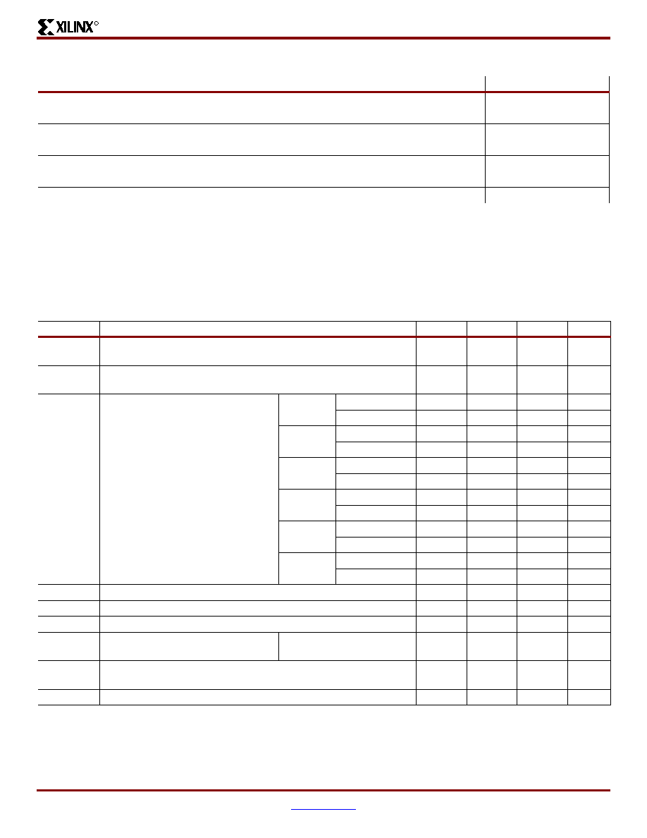
Recommended Operating Conditions
DC Characteristics Over Operating Conditions
Symbol
Description
Min
Max
Units
TJ
Junction temperature(1)
Commercial
0
85
°C
Industrial
–40
100
°C
VCCINT
Supply voltage relative to GND(2,5)
Commercial
2.5 – 5%
2.5 + 5%
V
Industrial
2.5 – 5%
2.5 + 5%
V
VCCO
Supply voltage relative to GND(3,5)
Commercial
1.4
3.6
V
Industrial
1.4
3.6
V
TIN
Input signal transition time(4)
-
250
ns
Notes:
1.
At junction temperatures above those listed as Operating Conditions, all delay parameters increase by 0.35% per
°C.
2.
Functional operation is guaranteed down to a minimum VCCINT of 2.25V (Nominal VCCINT – 10%). For every 50 mV reduction in
VCCINT below 2.375V (nominal VCCINT – 5%), all delay parameters increase by 3%.
3.
Minimum and maximum values for VCCO vary according to the I/O standard selected.
4.
Input and output measurement threshold is ~50% of VCCO. See "Delay Measurement Methodology," page 60 for specific levels.
5.
Supply voltages may be applied in any order desired.
Symbol
Description
Min
Typ
Max
Units
VDRINT
Data Retention VCCINT voltage (below which configuration data
may be lost)
2.0
-
V
VDRIO
Data Retention VCCO voltage (below which configuration data may
be lost)
1.2
-
V
ICCINTQ
Quiescent VCCINT supply current(1)
XC2S15
Commercial
-
10
30
mA
Industrial
-
10
60
mA
XC2S30
Commercial
-
10
30
mA
Industrial
-
10
60
mA
XC2S50
Commercial
-
12
50
mA
Industrial
-
12
100
mA
XC2S100
Commercial
-
12
50
mA
Industrial
-
12
100
mA
XC2S150
Commercial
-
15
50
mA
Industrial
-
15
100
mA
XC2S200
Commercial
-
15
75
mA
Industrial
-
15
150
mA
ICCOQ
Quiescent VCCO supply current(1)
--
2
mA
IREF
VREF current per VREF pin
-
20
μA
IL
Input or output leakage current(2)
–10
-
+10
μA
CIN
Input capacitance (sample tested)
VQ, CS, TQ, PQ, FG
packages
--
8
pF
IRPU
Pad pull-up (when selected) @ VIN = 0V, VCCO = 3.3V
(sample tested)(3)
--
0.25
mA
IRPD
Pad pull-down (when selected) @ VIN = 3.6V (sample tested)(3)
--
0.15
mA
Notes:
1.
With no output current loads, no active input pull-up resistors, all I/O pins 3-stated and floating.
2.
The I/O leakage current specification applies only when the VCCINT and VCCO supply voltages have reached their respective
minimum Recommended Operating Conditions.
3.
Internal pull-up and pull-down resistors guarantee valid logic levels at unconnected input pins. These pull-up and pull-down resistors
do not provide valid logic levels when input pins are connected to other circuits.
相关PDF资料 |
PDF描述 |
|---|---|
| XC2S100-5FG456I | IC FPGA 2.5V I-TEMP 456-FBGA |
| IDT71V35761S183PFG | IC SRAM 4MBIT 183MHZ 100TQFP |
| IDT71V35761S166PFG | IC SRAM 4MBIT 166MHZ 100TQFP |
| IDT71V424L15YG8 | IC SRAM 4MBIT 15NS 36SOJ |
| XCS40XL-4PQ240C | IC 3.3V FPGA COMM. TEMP 240PQFP |
相关代理商/技术参数 |
参数描述 |
|---|---|
| XC2S15-5CS144I | 功能描述:IC FPGA 2.5V I-TEMP 144-CSBGA RoHS:否 类别:集成电路 (IC) >> 嵌入式 - FPGA(现场可编程门阵列) 系列:Spartan®-II 产品变化通告:XC4000(E,L) Discontinuation 01/April/2002 标准包装:24 系列:XC4000E/X LAB/CLB数:100 逻辑元件/单元数:238 RAM 位总计:3200 输入/输出数:80 门数:3000 电源电压:4.5 V ~ 5.5 V 安装类型:表面贴装 工作温度:-40°C ~ 100°C 封装/外壳:120-BCBGA 供应商设备封装:120-CPGA(34.55x34.55) |
| XC2S15-5CSG144C | 制造商:XILINX 制造商全称:XILINX 功能描述:Spartan-II FPGA Family |
| XC2S15-5CSG144I | 制造商:XILINX 制造商全称:XILINX 功能描述:Spartan-II FPGA Family |
| XC2S15-5FG256C | 制造商:XILINX 制造商全称:XILINX 功能描述:Spartan-II FPGA Family |
| XC2S15-5FG256I | 制造商:XILINX 制造商全称:XILINX 功能描述:Spartan-II FPGA Family |
发布紧急采购,3分钟左右您将得到回复。