- 您现在的位置:买卖IC网 > PDF目录19312 > XC2S15-5VQG100C (Xilinx Inc)IC SPARTAN-II FPGA 15K 100-VQFP PDF资料下载
参数资料
| 型号: | XC2S15-5VQG100C |
| 厂商: | Xilinx Inc |
| 文件页数: | 11/99页 |
| 文件大小: | 0K |
| 描述: | IC SPARTAN-II FPGA 15K 100-VQFP |
| 标准包装: | 90 |
| 系列: | Spartan®-II |
| LAB/CLB数: | 96 |
| 逻辑元件/单元数: | 432 |
| RAM 位总计: | 16384 |
| 输入/输出数: | 60 |
| 门数: | 15000 |
| 电源电压: | 2.375 V ~ 2.625 V |
| 安装类型: | 表面贴装 |
| 工作温度: | 0°C ~ 85°C |
| 封装/外壳: | 100-TQFP |
| 供应商设备封装: | 100-VQFP(14x14) |
| 产品目录页面: | 599 (CN2011-ZH PDF) |
| 其它名称: | 122-1309 |
第1页第2页第3页第4页第5页第6页第7页第8页第9页第10页当前第11页第12页第13页第14页第15页第16页第17页第18页第19页第20页第21页第22页第23页第24页第25页第26页第27页第28页第29页第30页第31页第32页第33页第34页第35页第36页第37页第38页第39页第40页第41页第42页第43页第44页第45页第46页第47页第48页第49页第50页第51页第52页第53页第54页第55页第56页第57页第58页第59页第60页第61页第62页第63页第64页第65页第66页第67页第68页第69页第70页第71页第72页第73页第74页第75页第76页第77页第78页第79页第80页第81页第82页第83页第84页第85页第86页第87页第88页第89页第90页第91页第92页第93页第94页第95页第96页第97页第98页第99页
Spartan-II FPGA Family: Functional Description
DS001-2 (v2.8) June 13, 2008
Module 2 of 4
Product Specification
19
R
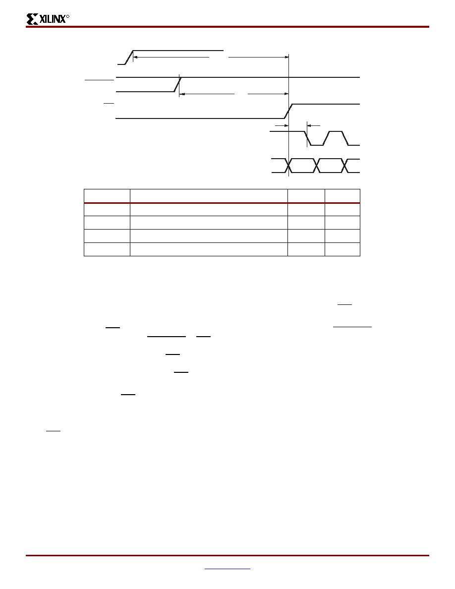
Clearing Configuration Memory
The device indicates that clearing the configuration memory
is in progress by driving INIT Low. At this time, the user can
delay configuration by holding either PROGRAM or INIT
Low, which causes the device to remain in the memory
clearing phase. Note that the bidirectional INIT line is
driving a Low logic level during memory clearing. To avoid
contention, use an open-drain driver to keep INIT Low.
With no delay in force, the device indicates that the memory
is completely clear by driving INIT High. The FPGA samples
its mode pins on this Low-to-High transition.
Loading Configuration Data
Once INIT is High, the user can begin loading configuration
data frames into the device. The details of loading the
configuration data are discussed in the sections treating the
configuration modes individually. The sequence of
operations necessary to load configuration data using the
serial modes is shown in Figure 14. Loading data using the
Slave Parallel mode is shown in Figure 19, page 25.
CRC Error Checking
During the loading of configuration data, a CRC value
embedded in the configuration file is checked against a
CRC value calculated within the FPGA. If the CRC values
do not match, the FPGA drives INIT Low to indicate that a
frame error has occurred and configuration is aborted.
To reconfigure the device, the PROGRAM pin should be
asserted to reset the configuration logic. Recycling power
also resets the FPGA for configuration. See "Clearing
Start-up
The start-up sequence oversees the transition of the FPGA
from the configuration state to full user operation. A match
of CRC values, indicating a successful loading of the
configuration data, initiates the sequence.
During start-up, the device performs four operations:
1.
The assertion of DONE. The failure of DONE to go High
may indicate the unsuccessful loading of configuration
data.
2.
The release of the Global Three State net. This
activates I/Os to which signals are assigned. The
remaining I/Os stay in a high-impedance state with
internal weak pull-down resistors present.
3.
Negates Global Set Reset (GSR). This allows all
flip-flops to change state.
4.
The assertion of Global Write Enable (GWE). This
allows all RAMs and flip-flops to change state.
Notes: (referring to waveform above:)
1.
Before configuration can begin, VCCINT must be greater than 1.6V and VCCO Bank 2 must be greater than 1.0V.
Figure 12: Configuration Timing on Power-Up
DS001_12_102301
TPOR
TPL
TICCK
Valid
CCLK Output or Input
M0, M1, M2
(Required)
PROGRAM
INIT
VCC(1)
.
Symbol
Description
Min
Max
TPOR
Power-on reset
-
2 ms
TPL
Program latency
-
100
μs
TICCK
CCLK output delay (Master Serial mode only)
0.5
μs4 μs
TPROGRAM
Program pulse width
300 ns
-
相关PDF资料 |
PDF描述 |
|---|---|
| EEM12DSXN | CONN EDGECARD 24POS DIP .156 SLD |
| RSA43DRMH | CONN EDGECARD 86POS .125 SQ WW |
| TACL335M004H | CAP TANT 3.3UF 4V 20% 0603 |
| KA79L05AZBU | IC REG LDO -5V .1A TO-92 |
| EEM12DSXH | CONN EDGECARD 24POS DIP .156 SLD |
相关代理商/技术参数 |
参数描述 |
|---|---|
| XC2S15-5VQG100I | 制造商:Xilinx 功能描述:FPGA SPARTAN-II 15K GATES 432 CELLS 263MHZ 2.5V 100VTQFP - Trays 制造商:Xilinx 功能描述:IC SYSTEM GATE |
| XC2S15-6CS144C | 功能描述:IC FPGA 2.5V C-TEMP 144-CSBGA RoHS:否 类别:集成电路 (IC) >> 嵌入式 - FPGA(现场可编程门阵列) 系列:Spartan®-II 产品变化通告:XC4000(E,L) Discontinuation 01/April/2002 标准包装:24 系列:XC4000E/X LAB/CLB数:100 逻辑元件/单元数:238 RAM 位总计:3200 输入/输出数:80 门数:3000 电源电压:4.5 V ~ 5.5 V 安装类型:表面贴装 工作温度:-40°C ~ 100°C 封装/外壳:120-BCBGA 供应商设备封装:120-CPGA(34.55x34.55) |
| XC2S15-6CS144I | 制造商:XILINX 制造商全称:XILINX 功能描述:Spartan-II FPGA Family |
| XC2S15-6CSG144C | 制造商:XILINX 制造商全称:XILINX 功能描述:Spartan-II FPGA Family |
| XC2S15-6CSG144I | 制造商:XILINX 制造商全称:XILINX 功能描述:Spartan-II FPGA Family |
发布紧急采购,3分钟左右您将得到回复。