参数资料
| 型号: | XC3S1000-5FTG256C |
| 厂商: | Xilinx Inc |
| 文件页数: | 216/272页 |
| 文件大小: | 0K |
| 描述: | SPARTAN-3A FPGA 1M 256-FTBGA |
| 产品培训模块: | Extended Spartan 3A FPGA Family |
| 标准包装: | 90 |
| 系列: | Spartan®-3 |
| LAB/CLB数: | 1920 |
| 逻辑元件/单元数: | 17280 |
| RAM 位总计: | 442368 |
| 输入/输出数: | 173 |
| 门数: | 1000000 |
| 电源电压: | 1.14 V ~ 1.26 V |
| 安装类型: | 表面贴装 |
| 工作温度: | 0°C ~ 85°C |
| 封装/外壳: | 256-LBGA |
| 供应商设备封装: | 256-FTBGA |
| 配用: | 122-1502-ND - KIT STARTER SPARTAN-3 PCI-E |
第1页第2页第3页第4页第5页第6页第7页第8页第9页第10页第11页第12页第13页第14页第15页第16页第17页第18页第19页第20页第21页第22页第23页第24页第25页第26页第27页第28页第29页第30页第31页第32页第33页第34页第35页第36页第37页第38页第39页第40页第41页第42页第43页第44页第45页第46页第47页第48页第49页第50页第51页第52页第53页第54页第55页第56页第57页第58页第59页第60页第61页第62页第63页第64页第65页第66页第67页第68页第69页第70页第71页第72页第73页第74页第75页第76页第77页第78页第79页第80页第81页第82页第83页第84页第85页第86页第87页第88页第89页第90页第91页第92页第93页第94页第95页第96页第97页第98页第99页第100页第101页第102页第103页第104页第105页第106页第107页第108页第109页第110页第111页第112页第113页第114页第115页第116页第117页第118页第119页第120页第121页第122页第123页第124页第125页第126页第127页第128页第129页第130页第131页第132页第133页第134页第135页第136页第137页第138页第139页第140页第141页第142页第143页第144页第145页第146页第147页第148页第149页第150页第151页第152页第153页第154页第155页第156页第157页第158页第159页第160页第161页第162页第163页第164页第165页第166页第167页第168页第169页第170页第171页第172页第173页第174页第175页第176页第177页第178页第179页第180页第181页第182页第183页第184页第185页第186页第187页第188页第189页第190页第191页第192页第193页第194页第195页第196页第197页第198页第199页第200页第201页第202页第203页第204页第205页第206页第207页第208页第209页第210页第211页第212页第213页第214页第215页当前第216页第217页第218页第219页第220页第221页第222页第223页第224页第225页第226页第227页第228页第229页第230页第231页第232页第233页第234页第235页第236页第237页第238页第239页第240页第241页第242页第243页第244页第245页第246页第247页第248页第249页第250页第251页第252页第253页第254页第255页第256页第257页第258页第259页第260页第261页第262页第263页第264页第265页第266页第267页第268页第269页第270页第271页第272页
Spartan-3 FPGA Family: Functional Description
DS099 (v3.1) June 27, 2013
Product Specification
48
Slave Serial mode is selected by applying <111> to the mode pins (M0, M1, and M2). A pull-up on the mode pins makes
slave serial the default mode if the pins are left unconnected.
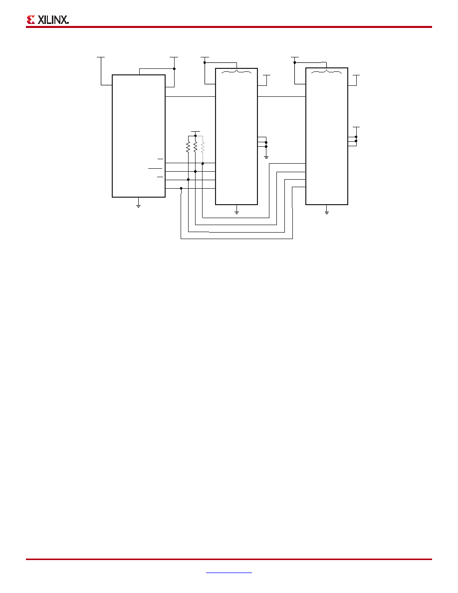
Master Serial Mode
In Master Serial mode, the FPGA drives CCLK pin, which behaves as a bidirectional I/O pin. The FPGA in the center of
Figure 26 is set for Master Serial mode and connects to the serial configuration PROM and to the CCLK inputs of any slave
FPGAs in a configuration daisy-chain. The master FPGA drives the configuration clock on the CCLK pin to the Xilinx Serial
PROM, which, in response, provides bit-serial data to the FPGA’s DIN input. The FPGA accepts this data on each rising
CCLK edge. After the master FPGA finishes configuring, it passes data on its DOUT pin to the next FPGA device in a
daisy-chain. The DOUT data appears after the falling CCLK clock edge.
The Master Serial mode interface is identical to Slave Serial except that an internal oscillator generates the configuration
clock (CCLK). A wide range of frequencies can be selected for CCLK, which always starts at a default frequency of 6 MHz.
Configuration bits then switch CCLK to a higher frequency for the remainder of the configuration.
Slave Parallel Mode (SelectMAP)
The Parallel or SelectMAP modes support the fastest configuration. Byte-wide data is written into the FPGA with a BUSY
flag controlling the flow of data. An external source provides 8-bit-wide data, CCLK, an active-Low Chip Select (CS_B) signal
and an active-Low Write signal (RDWR_B). If BUSY is asserted (High) by the FPGA, the data must be held until BUSY goes
Low. Data can also be read using the Slave Parallel mode. If RDWR_B is asserted, configuration data is read out of the
FPGA as part of a readback operation.
After configuration, it is possible to use any of the Multipurpose pins (DIN/D0-D7, DOUT/BUSY, INIT_B, CS_B, and
RDWR_B) as User I/Os. To do this, simply set the BitGen option Persist to No and assign the desired signals to multipurpose
configuration pins using the Xilinx development software. Alternatively, it is possible to continue using the configuration port
X-Ref Target - Figure 26
Figure 26: Connection Diagram for Master and Slave Serial Configuration
Notes:
1.
There are two ways to use the DONE line. First, one may set the BitGen option DriveDone to "Yes" only for the last
FPGA to be configured in the chain shown above (or for the single FPGA as may be the case). This enables the DONE
pin to drive High; thus, no pull-up resistor is necessary. DriveDone is set to "No" for the remaining FPGAs in the chain.
Second, DriveDone can be set to "No" for all FPGAs. Then all DONE lines are open-drain and require the pull-up
resistor shown in grey. In most cases, a value between 3.3K
Ω to 4.7KΩ is sufficient. However, when using DONE
synchronously with a long chain of FPGAs, cumulative capacitance may necessitate lower resistor values (e.g. down
to 330
Ω) in order to ensure a rise time within one clock cycle.
2.
For information on how to program the FPGA using 3.3V signals and power, see 3.3V-Tolerant Configuration Interface.
DOUT
DIN
CCLK
DONE
INIT_B
Spartan-3
FPGA
Master
PROG_B
DIN
CCLK
DONE
INIT_B
Spartan-3
FPGA
Slave
PROG_B
DS099_23_112905
D0
CLK
CE
OE/RESET
CF
Platform
Flash PROM
XCF0xS
or
XCFxxP
VCCINT
1.2V
VCCAUX
VCCO Bank 4
2.5V
4.7K
Ω
All
2.5V
VCCAUX
VCCINT
VCCO Bank 4
1.2V
1.8V: XCFxxP
VCCINT
VCCJ
VCCO
2.5V
M0
M1
M2
M0
M1
M2
GND
3.3V: XCF0xS
相关PDF资料 |
PDF描述 |
|---|---|
| XC2V40-4FG256I | IC FPGA VIRTEX-II 256FGBGA |
| XC2V40-5FGG256C | IC FPGA VIRTEX-II 40K 256-FBGA |
| XC2V40-4FGG256I | IC FPGA VIRTEX-II 40K 256-FBGA |
| 3341-32BULK | CONN JACKSOCKET M2.5/4-40 0.50" |
| DB53750-2 | DSUB DB INTERFACIAL SEAL |
相关代理商/技术参数 |
参数描述 |
|---|---|
| XC3S1000-5PQ208C | 制造商:XILINX 制造商全称:XILINX 功能描述:Spartan-3 FPGA |
| XC3S1000-5PQ208I | 制造商:XILINX 制造商全称:XILINX 功能描述:Spartan-3 FPGA |
| XC3S1000-5PQG208C | 制造商:XILINX 制造商全称:XILINX 功能描述:Spartan-3 FPGA Family: Complete Data Sheet |
| XC3S1000-5PQG208I | 制造商:XILINX 制造商全称:XILINX 功能描述:Spartan-3 FPGA Family: Complete Data Sheet |
| XC3S1000-5TQ144C | 制造商:XILINX 制造商全称:XILINX 功能描述:Spartan-3 FPGA |
发布紧急采购,3分钟左右您将得到回复。