参数资料
| 型号: | XC3S1500-5FGG456C |
| 厂商: | Xilinx Inc |
| 文件页数: | 219/272页 |
| 文件大小: | 0K |
| 描述: | SPARTAN-3A FPGA 1.5M 456-FBGA |
| 产品培训模块: | Extended Spartan 3A FPGA Family |
| 标准包装: | 60 |
| 系列: | Spartan®-3 |
| LAB/CLB数: | 3328 |
| 逻辑元件/单元数: | 29952 |
| RAM 位总计: | 589824 |
| 输入/输出数: | 333 |
| 门数: | 1500000 |
| 电源电压: | 1.14 V ~ 1.26 V |
| 安装类型: | 表面贴装 |
| 工作温度: | 0°C ~ 85°C |
| 封装/外壳: | 456-BBGA |
| 供应商设备封装: | 456-FBGA |
| 配用: | NANO-SPARTAN-ND - KIT NANOBOARD AND SPARTAN3 DC 807-1001-ND - DAUGHTER CARD XILINX SPARTAN 3 |
第1页第2页第3页第4页第5页第6页第7页第8页第9页第10页第11页第12页第13页第14页第15页第16页第17页第18页第19页第20页第21页第22页第23页第24页第25页第26页第27页第28页第29页第30页第31页第32页第33页第34页第35页第36页第37页第38页第39页第40页第41页第42页第43页第44页第45页第46页第47页第48页第49页第50页第51页第52页第53页第54页第55页第56页第57页第58页第59页第60页第61页第62页第63页第64页第65页第66页第67页第68页第69页第70页第71页第72页第73页第74页第75页第76页第77页第78页第79页第80页第81页第82页第83页第84页第85页第86页第87页第88页第89页第90页第91页第92页第93页第94页第95页第96页第97页第98页第99页第100页第101页第102页第103页第104页第105页第106页第107页第108页第109页第110页第111页第112页第113页第114页第115页第116页第117页第118页第119页第120页第121页第122页第123页第124页第125页第126页第127页第128页第129页第130页第131页第132页第133页第134页第135页第136页第137页第138页第139页第140页第141页第142页第143页第144页第145页第146页第147页第148页第149页第150页第151页第152页第153页第154页第155页第156页第157页第158页第159页第160页第161页第162页第163页第164页第165页第166页第167页第168页第169页第170页第171页第172页第173页第174页第175页第176页第177页第178页第179页第180页第181页第182页第183页第184页第185页第186页第187页第188页第189页第190页第191页第192页第193页第194页第195页第196页第197页第198页第199页第200页第201页第202页第203页第204页第205页第206页第207页第208页第209页第210页第211页第212页第213页第214页第215页第216页第217页第218页当前第219页第220页第221页第222页第223页第224页第225页第226页第227页第228页第229页第230页第231页第232页第233页第234页第235页第236页第237页第238页第239页第240页第241页第242页第243页第244页第245页第246页第247页第248页第249页第250页第251页第252页第253页第254页第255页第256页第257页第258页第259页第260页第261页第262页第263页第264页第265页第266页第267页第268页第269页第270页第271页第272页
Spartan-3 FPGA Family: Functional Description
DS099 (v3.1) June 27, 2013
Product Specification
50
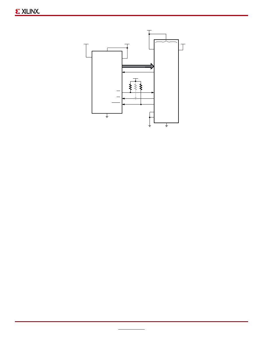
Master Parallel Mode
In this mode, the FPGA configures from byte-wide data, and the FPGA supplies the CCLK configuration clock. In Master
configuration modes, CCLK behaves as a bidirectional I/O pin. Timing is similar to the Slave Parallel mode except that CCLK
is supplied by the FPGA. The device connections are shown in Figure 28.
Boundary-Scan (JTAG) Mode
In Boundary-Scan mode, dedicated pins are used for configuring the FPGA. The configuration is done entirely through the
IEEE 1149.1 Test Access Port (TAP). FPGA configuration using the Boundary-Scan mode is compatible with the IEEE Std
1149.1-1993 standard and IEEE Std 1532 for In-System Configurable (ISC) devices.
Configuration through the boundary-scan port is always available, regardless of the selected configuration mode. In some
cases, however, the mode pin setting may affect proper programming of the device due to various interactions. For example,
if the mode pins are set to Master Serial or Master Parallel mode, and the associated PROM is already programmed with a
valid configuration image, then there is potential for configuration interference between the JTAG and PROM data. Selecting
the Boundary-Scan mode disables the other modes and is the most reliable mode when programming via JTAG.
Configuration Sequence
The configuration of Spartan-3 devices is a three-stage process that occurs after Power-On Reset or the assertion of
PROG_B. POR occurs after the VCCINT, VCCAUX, and VCCO Bank 4 supplies have reached their respective maximum input
threshold levels (see Table 29, page 59). After POR, the three-stage process begins.
First, the configuration memory is cleared. Next, configuration data is loaded into the memory, and finally, the logic is
activated by a start-up process. A flow diagram for the configuration sequence of the Serial and Parallel modes is shown in
Figure 29. The flow diagram for the Boundary-Scan configuration sequence appears in Figure 30.
X-Ref Target - Figure 28
Figure 28: Connection Diagram for Master Parallel Configuration
Spartan-3
Master
D[0:7]
CCLK
PROG_B
DONE
INIT_B
DATA[0:7]
CCLK
RDWR_B
CS_B
CF
CE
OE/RESET
Platform Flash
PROM
DS099_25_112905
2.5V
VCCAUX
VCCO Banks 4 & 5
VCCINT
1.2V
GND
1.8V
VCCINT
VCCJ
VCCO
2.5V
XCFxxP
2.5V
All
4.7K
Ω
Notes:
1.
There are two ways to use the DONE line. First, one may set the BitGen option DriveDone to "Yes" only for
the last FPGA to be configured in the chain shown above (or for the single FPGA as may be the case). This
enables the DONE pin to drive High; thus, no pull-up resistor is necessary. DriveDone is set to "No" for the
remaining FPGAs in the chain. Second, DriveDone can be set to "No" for all FPGAs. Then all DONE lines
are open-drain and require the pull-up resistor shown in grey. In most cases, a value between 3.3K
Ω to
4.7K
Ω is sufficient. However, when using DONE synchronously with a long chain of FPGAs, cumulative
capacitance may necessitate lower resistor values (e.g. down to 330
Ω) in order to ensure a rise time within
one clock cycle.
相关PDF资料 |
PDF描述 |
|---|---|
| 25C040T-E/SN | IC EEPROM 4KBIT 3MHZ 8SOIC |
| XCV50E-8CS144C | IC FPGA 1.8V C-TEMP 144-CSBGA |
| RMC65DRYI-S13 | CONN EDGECARD 130PS DIP .100 SLD |
| XC3S1600E-4FG320I | IC FPGA SPARTAN 3E 320FBGA |
| AMC40DRTS | CONN EDGECARD 80POS .100 DIP SLD |
相关代理商/技术参数 |
参数描述 |
|---|---|
| XC3S1500-5FGG676C | 功能描述:SPARTAN-3A FPGA 1.5M 676-FBGA RoHS:是 类别:集成电路 (IC) >> 嵌入式 - FPGA(现场可编程门阵列) 系列:Spartan®-3 产品变化通告:Step Intro and Pkg Change 11/March/2008 标准包装:1 系列:Virtex®-5 SXT LAB/CLB数:4080 逻辑元件/单元数:52224 RAM 位总计:4866048 输入/输出数:480 门数:- 电源电压:0.95 V ~ 1.05 V 安装类型:表面贴装 工作温度:-40°C ~ 100°C 封装/外壳:1136-BBGA,FCBGA 供应商设备封装:1136-FCBGA 配用:568-5088-ND - BOARD DEMO DAC1408D750122-1796-ND - EVALUATION PLATFORM VIRTEX-5 |
| XC3S1500-5FT256C | 制造商:XILINX 制造商全称:XILINX 功能描述:Spartan-3 FPGA |
| XC3S1500-5FT256I | 制造商:XILINX 制造商全称:XILINX 功能描述:Spartan-3 FPGA |
| XC3S1500-5PQ208C | 制造商:XILINX 制造商全称:XILINX 功能描述:Spartan-3 FPGA |
| XC3S1500-5PQ208I | 制造商:XILINX 制造商全称:XILINX 功能描述:Spartan-3 FPGA |
发布紧急采购,3分钟左右您将得到回复。