参数资料
| 型号: | XC3S1600E-4FGG320I |
| 厂商: | Xilinx Inc |
| 文件页数: | 40/227页 |
| 文件大小: | 0K |
| 描述: | IC FPGA SPARTAN-3E 1600K 320FBGA |
| 标准包装: | 84 |
| 系列: | Spartan®-3E |
| LAB/CLB数: | 3688 |
| 逻辑元件/单元数: | 33192 |
| RAM 位总计: | 663552 |
| 输入/输出数: | 250 |
| 门数: | 1600000 |
| 电源电压: | 1.14 V ~ 1.26 V |
| 安装类型: | 表面贴装 |
| 工作温度: | -40°C ~ 100°C |
| 封装/外壳: | 320-BGA |
| 供应商设备封装: | 320-FBGA(19x19) |
| 配用: | HW-XA3S1600E-UNI-G-ND - KIT DEVELOPMENT AUTOMOTIVE ECU |
第1页第2页第3页第4页第5页第6页第7页第8页第9页第10页第11页第12页第13页第14页第15页第16页第17页第18页第19页第20页第21页第22页第23页第24页第25页第26页第27页第28页第29页第30页第31页第32页第33页第34页第35页第36页第37页第38页第39页当前第40页第41页第42页第43页第44页第45页第46页第47页第48页第49页第50页第51页第52页第53页第54页第55页第56页第57页第58页第59页第60页第61页第62页第63页第64页第65页第66页第67页第68页第69页第70页第71页第72页第73页第74页第75页第76页第77页第78页第79页第80页第81页第82页第83页第84页第85页第86页第87页第88页第89页第90页第91页第92页第93页第94页第95页第96页第97页第98页第99页第100页第101页第102页第103页第104页第105页第106页第107页第108页第109页第110页第111页第112页第113页第114页第115页第116页第117页第118页第119页第120页第121页第122页第123页第124页第125页第126页第127页第128页第129页第130页第131页第132页第133页第134页第135页第136页第137页第138页第139页第140页第141页第142页第143页第144页第145页第146页第147页第148页第149页第150页第151页第152页第153页第154页第155页第156页第157页第158页第159页第160页第161页第162页第163页第164页第165页第166页第167页第168页第169页第170页第171页第172页第173页第174页第175页第176页第177页第178页第179页第180页第181页第182页第183页第184页第185页第186页第187页第188页第189页第190页第191页第192页第193页第194页第195页第196页第197页第198页第199页第200页第201页第202页第203页第204页第205页第206页第207页第208页第209页第210页第211页第212页第213页第214页第215页第216页第217页第218页第219页第220页第221页第222页第223页第224页第225页第226页第227页
Spartan-3E FPGA Family: DC and Switching Characteristics
DS312 (v4.1) July 19, 2013
Product Specification
134
Simultaneously Switching Output Guidelines
This section provides guidelines for the recommended
maximum allowable number of Simultaneous Switching
Outputs (SSOs). These guidelines describe the maximum
number of user I/O pins of a given output signal standard
that should simultaneously switch in the same direction,
while maintaining a safe level of switching noise. Meeting
these guidelines for the stated test conditions ensures that
the FPGA operates free from the adverse effects of ground
and power bounce.
Ground or power bounce occurs when a large number of
outputs simultaneously switch in the same direction. The
output drive transistors all conduct current to a common
voltage rail. Low-to-High transitions conduct to the VCCO
rail; High-to-Low transitions conduct to the GND rail. The
resulting cumulative current transient induces a voltage
difference across the inductance that exists between the die
pad and the power supply or ground return. The inductance
is associated with bonding wires, the package lead frame,
and any other signal routing inside the package. Other
variables contribute to SSO noise levels, including stray
inductance on the PCB as well as capacitive loading at
receivers. Any SSO-induced voltage consequently affects
internal switching noise margins and ultimately signal
quality.
guidelines. For each device/package combination, Table 96
provides the number of equivalent VCCO/GND pairs. The
equivalent number of pairs is based on characterization and
might not match the physical number of pairs. For each
output signal standard and drive strength, Table 97
recommends the maximum number of SSOs, switching in
the same direction, allowed per VCCO/GND pair within an
I/O bank. The guidelines in Table 97 are categorized by
package style. Multiply the appropriate numbers from
SSOs allowed within an I/O bank. Exceeding these SSO
guidelines might result in increased power or ground
bounce, degraded signal integrity, or increased system jitter.
The recommended maximum SSO values assumes that the
FPGA is soldered on the printed circuit board and that the
board uses sound design practices. The SSO values do not
apply for FPGAs mounted in sockets, due to the lead
inductance introduced by the socket.
The number of SSOs allowed for quad-flat packages (VQ,
TQ, PQ) is lower than for ball grid array packages (FG) due
to the larger lead inductance of the quad-flat packages. The
results for chip-scale packaging (CP132) are better than
quad-flat packaging but not as high as for ball grid array
packaging. Ball grid array packages are recommended for
applications with a large number of simultaneously
switching outputs.
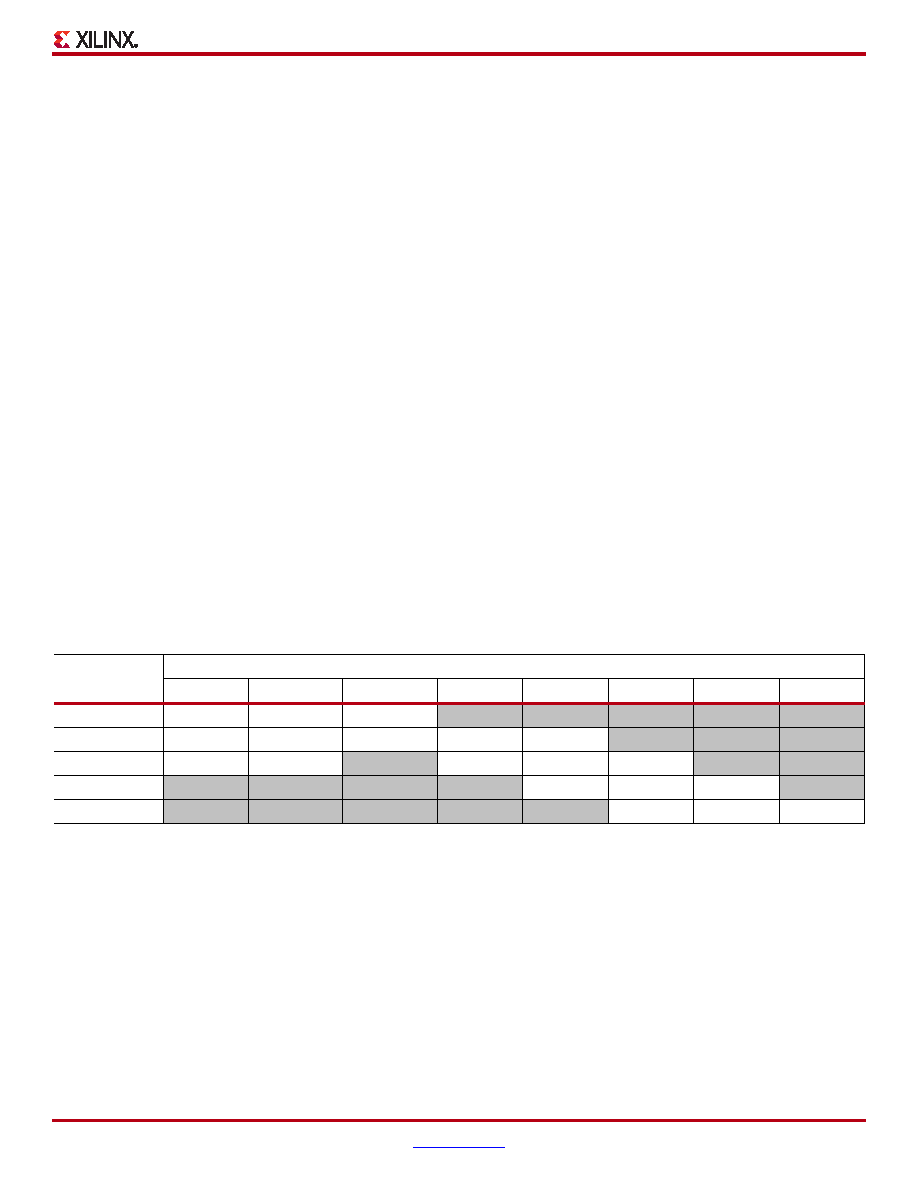
Table 96: Equivalent VCCO/GND Pairs per Bank
Device
Package Style (including Pb-free)
VQ100
CP132
TQ144
PQ208
FT256
FG320
FG400
FG484
XC3S100E
2
-
XC3S250E
2
3
4
-
XC3S500E
2
-
345
-
XC3S1200E
-
4
5
6
-
XC3S1600E
-
-5
6
7
相关PDF资料 |
PDF描述 |
|---|---|
| XA3S1000-4FGG456Q | IC FPGA SPARTAN-3 1M 456-FBGA |
| GCB108DHBN | CONN EDGECARD 216PS R/A .050 SLD |
| GCB108DHBD | CONN EDGECARD 216PS R/A .050 SLD |
| XA6SLX45T-2CSG324I | IC FPGA SPARTAN 6 43K 324CSGBGA |
| XC6SLX45T-N3CSG324I | IC FPGA SPARTAN-6 324CSBGA |
相关代理商/技术参数 |
参数描述 |
|---|---|
| XC3S1600E-4FGG400C | 功能描述:IC SPARTAN-3E FPGA 1600K 400FBGA RoHS:是 类别:集成电路 (IC) >> 嵌入式 - FPGA(现场可编程门阵列) 系列:Spartan®-3E 标准包装:60 系列:XP LAB/CLB数:- 逻辑元件/单元数:10000 RAM 位总计:221184 输入/输出数:244 门数:- 电源电压:1.71 V ~ 3.465 V 安装类型:表面贴装 工作温度:0°C ~ 85°C 封装/外壳:388-BBGA 供应商设备封装:388-FPBGA(23x23) 其它名称:220-1241 |
| XC3S1600E-4FGG400I | 功能描述:IC FPGA SPARTAN-3E 1600K 400FBGA RoHS:是 类别:集成电路 (IC) >> 嵌入式 - FPGA(现场可编程门阵列) 系列:Spartan®-3E 标准包装:40 系列:Spartan® 6 LX LAB/CLB数:3411 逻辑元件/单元数:43661 RAM 位总计:2138112 输入/输出数:358 门数:- 电源电压:1.14 V ~ 1.26 V 安装类型:表面贴装 工作温度:-40°C ~ 100°C 封装/外壳:676-BGA 供应商设备封装:676-FBGA(27x27) |
| XC3S1600E-4FGG484C | 制造商:Xilinx 功能描述:FPGA SPARTAN-3E 1.6M GATES 33192 CELLS 572MHZ 90NM 1.2V 484F - Trays 制造商:Xilinx 功能描述:FPGA SPARTAN-3E 1600K GATES 484FBGA |
| XC3S1600E-4FGG484I | 功能描述:IC FPGA SPARTAN-3E 1600K 484FBGA RoHS:是 类别:集成电路 (IC) >> 嵌入式 - FPGA(现场可编程门阵列) 系列:Spartan®-3E 产品变化通告:Step Intro and Pkg Change 11/March/2008 标准包装:1 系列:Virtex®-5 SXT LAB/CLB数:4080 逻辑元件/单元数:52224 RAM 位总计:4866048 输入/输出数:480 门数:- 电源电压:0.95 V ~ 1.05 V 安装类型:表面贴装 工作温度:-40°C ~ 100°C 封装/外壳:1136-BBGA,FCBGA 供应商设备封装:1136-FCBGA 配用:568-5088-ND - BOARD DEMO DAC1408D750122-1796-ND - EVALUATION PLATFORM VIRTEX-5 |
| XC3S1600E-4FT256C | 制造商:XILINX 制造商全称:XILINX 功能描述:Spartan-3E FPGA Family |
发布紧急采购,3分钟左右您将得到回复。