- 您现在的位置:买卖IC网 > PDF目录19312 > XC3S200-4VQG100I (Xilinx Inc)SPARTAN-3 FPGA 200K STD 100VQFP PDF资料下载
参数资料
| 型号: | XC3S200-4VQG100I |
| 厂商: | Xilinx Inc |
| 文件页数: | 46/272页 |
| 文件大小: | 0K |
| 描述: | SPARTAN-3 FPGA 200K STD 100VQFP |
| 产品培训模块: | Extended Spartan 3A FPGA Family |
| 标准包装: | 90 |
| 系列: | Spartan®-3 |
| LAB/CLB数: | 480 |
| 逻辑元件/单元数: | 4320 |
| RAM 位总计: | 221184 |
| 输入/输出数: | 63 |
| 门数: | 200000 |
| 电源电压: | 1.14 V ~ 1.26 V |
| 安装类型: | 表面贴装 |
| 工作温度: | -40°C ~ 100°C |
| 封装/外壳: | 100-TQFP |
| 供应商设备封装: | 100-VQFP(14x14) |
| 其它名称: | 122-1712 XC3S200-4VQG100I-ND |
第1页第2页第3页第4页第5页第6页第7页第8页第9页第10页第11页第12页第13页第14页第15页第16页第17页第18页第19页第20页第21页第22页第23页第24页第25页第26页第27页第28页第29页第30页第31页第32页第33页第34页第35页第36页第37页第38页第39页第40页第41页第42页第43页第44页第45页当前第46页第47页第48页第49页第50页第51页第52页第53页第54页第55页第56页第57页第58页第59页第60页第61页第62页第63页第64页第65页第66页第67页第68页第69页第70页第71页第72页第73页第74页第75页第76页第77页第78页第79页第80页第81页第82页第83页第84页第85页第86页第87页第88页第89页第90页第91页第92页第93页第94页第95页第96页第97页第98页第99页第100页第101页第102页第103页第104页第105页第106页第107页第108页第109页第110页第111页第112页第113页第114页第115页第116页第117页第118页第119页第120页第121页第122页第123页第124页第125页第126页第127页第128页第129页第130页第131页第132页第133页第134页第135页第136页第137页第138页第139页第140页第141页第142页第143页第144页第145页第146页第147页第148页第149页第150页第151页第152页第153页第154页第155页第156页第157页第158页第159页第160页第161页第162页第163页第164页第165页第166页第167页第168页第169页第170页第171页第172页第173页第174页第175页第176页第177页第178页第179页第180页第181页第182页第183页第184页第185页第186页第187页第188页第189页第190页第191页第192页第193页第194页第195页第196页第197页第198页第199页第200页第201页第202页第203页第204页第205页第206页第207页第208页第209页第210页第211页第212页第213页第214页第215页第216页第217页第218页第219页第220页第221页第222页第223页第224页第225页第226页第227页第228页第229页第230页第231页第232页第233页第234页第235页第236页第237页第238页第239页第240页第241页第242页第243页第244页第245页第246页第247页第248页第249页第250页第251页第252页第253页第254页第255页第256页第257页第258页第259页第260页第261页第262页第263页第264页第265页第266页第267页第268页第269页第270页第271页第272页
Spartan-3 FPGA Family: Functional Description
DS099 (v3.1) June 27, 2013
Product Specification
14
ESD Protection
Clamp diodes protect all device pads against damage from Electro-Static Discharge (ESD) as well as excessive voltage
transients. Each I/O has two clamp diodes: One diode extends P-to-N from the pad to VCCO and a second diode extends
N-to-P from the pad to GND. During operation, these diodes are normally biased in the off state. These clamp diodes are
always connected to the pad, regardless of the signal standard selected. The presence of diodes limits the ability of
Spartan-3 FPGA I/Os to tolerate high signal voltages. The VIN absolute maximum rating in Table 28, page 58 specifies the
voltage range that I/Os can tolerate.
Slew Rate Control and Drive Strength
Two options, FAST and SLOW, control the output slew rate. The FAST option supports output switching at a high rate. The
SLOW option reduces bus transients. These options are only available when using one of the LVCMOS or LVTTL standards,
which also provide up to seven different levels of current drive strength: 2, 4, 6, 8, 12, 16, and 24 mA. Choosing the
appropriate drive strength level is yet another means to minimize bus transients.
Table 7 shows the drive strengths that the LVCMOS and LVTTL standards support.
Boundary-Scan Capability
All Spartan-3 FPGA IOBs support boundary-scan testing compatible with IEEE 1149.1 standards. During boundary- scan
operations such as EXTEST and HIGHZ the I/O pull-down resistor is active. For more information, see Boundary-Scan
(JTAG) Mode, page 50, and refer to the “Using Boundary-Scan and BSDL Files” chapter in UG331.
SelectIO Interface Signal Standards
The IOBs support 18 different single-ended signal standards, as listed in Table 8. Furthermore, the majority of IOBs can be
used in specific pairs supporting any of eight differential signal standards, as shown in Table 9.
To define the SelectIO interface signaling standard in a design, set the IOSTANDARD attribute to the appropriate setting.
Xilinx provides a variety of different methods for applying the IOSTANDARD for maximum flexibility. For a full description of
different methods of applying attributes to control IOSTANDARD, refer to the “Using I/O Resources” chapter in UG331.
Together with placing the appropriate I/O symbol, two externally applied voltage levels, VCCO and VREF, select the desired
signal standard. The VCCO lines provide current to the output driver. The voltage on these lines determines the output
voltage swing for all standards except GTL and GTLP.
All single-ended standards except the LVCMOS, LVTTL, and PCI varieties require a Reference Voltage (VREF) to bias the
input-switching threshold. Once a configuration data file is loaded into the FPGA that calls for the I/Os of a given bank to use
such a signal standard, a few specifically reserved I/O pins on the same bank automatically convert to VREF inputs. When
using one of the LVCMOS standards, these pins remain I/Os because the VCCO voltage biases the input-switching
threshold, so there is no need for VREF. Select the VCCO and VREF levels to suit the desired single-ended standard according
to Table 8.
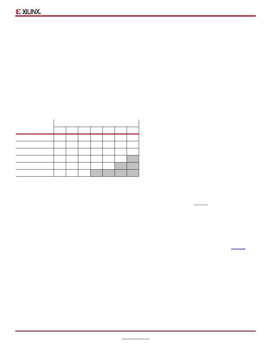
Table 7: Programmable Output Drive Current
Signal Standard
(IOSTANDARD)
Current Drive (mA)
2468
12
16
24
LVTTL
LVCMOS33
LVCMOS25
LVCMOS18
–
LVCMOS15
–
LVCMOS12
–
相关PDF资料 |
PDF描述 |
|---|---|
| XC3S200A-4VQG100I | IC FPGA SPARTAN-3A 200K 100-VQFP |
| GBM10DCSN | CONN EDGECARD 20POS DIP .156 SLD |
| GBM10DCSH | CONN EDGECARD 20POS DIP .156 SLD |
| RMA43DRMN | CONN EDGECARD 86POS .125 SQ WW |
| GBM10DCSD | CONN EDGECARD 20POS DIP .156 SLD |
相关代理商/技术参数 |
参数描述 |
|---|---|
| XC3S200-5CP132C | 制造商:XILINX 制造商全称:XILINX 功能描述:Spartan-3 FPGA |
| XC3S200-5CP132I | 制造商:XILINX 制造商全称:XILINX 功能描述:Spartan-3 FPGA |
| XC3S200-5CPG132C | 制造商:XILINX 制造商全称:XILINX 功能描述:Spartan-3 FPGA Family: Complete Data Sheet |
| XC3S200-5CPG132I | 制造商:XILINX 制造商全称:XILINX 功能描述:Spartan-3 FPGA Family: Complete Data Sheet |
| XC3S200-5FG1156C | 制造商:XILINX 制造商全称:XILINX 功能描述:Spartan-3 FPGA |
发布紧急采购,3分钟左右您将得到回复。