参数资料
| 型号: | XC3S2000-4FGG900I |
| 厂商: | Xilinx Inc |
| 文件页数: | 57/272页 |
| 文件大小: | 0K |
| 描述: | SPARTAN-3A FPGA 2M STD 900-FBGA |
| 产品培训模块: | Extended Spartan 3A FPGA Family |
| 标准包装: | 27 |
| 系列: | Spartan®-3 |
| LAB/CLB数: | 5120 |
| 逻辑元件/单元数: | 46080 |
| RAM 位总计: | 737280 |
| 输入/输出数: | 565 |
| 门数: | 2000000 |
| 电源电压: | 1.14 V ~ 1.26 V |
| 安装类型: | 表面贴装 |
| 工作温度: | -40°C ~ 100°C |
| 封装/外壳: | 900-BBGA |
| 供应商设备封装: | 900-FBGA |
第1页第2页第3页第4页第5页第6页第7页第8页第9页第10页第11页第12页第13页第14页第15页第16页第17页第18页第19页第20页第21页第22页第23页第24页第25页第26页第27页第28页第29页第30页第31页第32页第33页第34页第35页第36页第37页第38页第39页第40页第41页第42页第43页第44页第45页第46页第47页第48页第49页第50页第51页第52页第53页第54页第55页第56页当前第57页第58页第59页第60页第61页第62页第63页第64页第65页第66页第67页第68页第69页第70页第71页第72页第73页第74页第75页第76页第77页第78页第79页第80页第81页第82页第83页第84页第85页第86页第87页第88页第89页第90页第91页第92页第93页第94页第95页第96页第97页第98页第99页第100页第101页第102页第103页第104页第105页第106页第107页第108页第109页第110页第111页第112页第113页第114页第115页第116页第117页第118页第119页第120页第121页第122页第123页第124页第125页第126页第127页第128页第129页第130页第131页第132页第133页第134页第135页第136页第137页第138页第139页第140页第141页第142页第143页第144页第145页第146页第147页第148页第149页第150页第151页第152页第153页第154页第155页第156页第157页第158页第159页第160页第161页第162页第163页第164页第165页第166页第167页第168页第169页第170页第171页第172页第173页第174页第175页第176页第177页第178页第179页第180页第181页第182页第183页第184页第185页第186页第187页第188页第189页第190页第191页第192页第193页第194页第195页第196页第197页第198页第199页第200页第201页第202页第203页第204页第205页第206页第207页第208页第209页第210页第211页第212页第213页第214页第215页第216页第217页第218页第219页第220页第221页第222页第223页第224页第225页第226页第227页第228页第229页第230页第231页第232页第233页第234页第235页第236页第237页第238页第239页第240页第241页第242页第243页第244页第245页第246页第247页第248页第249页第250页第251页第252页第253页第254页第255页第256页第257页第258页第259页第260页第261页第262页第263页第264页第265页第266页第267页第268页第269页第270页第271页第272页
Spartan-3 FPGA Family: Functional Description
DS099 (v3.1) June 27, 2013
Product Specification
15
Differential standards employ a pair of signals, one the opposite polarity of the other. The noise canceling (e.g.,
Common-Mode Rejection) properties of these standards permit exceptionally high data transfer rates. This section
introduces the differential signaling capabilities of Spartan-3 devices.
Each device-package combination designates specific I/O pairs that are specially optimized to support differential
standards. A unique “L-number”, part of the pin name, identifies the line-pairs associated with each bank (see Figure 40,
page 112). For each pair, the letters ‘P’ and ‘N’ designate the true and inverted lines, respectively. For example, the pin
names IO_L43P_7 and IO_L43N_7 indicate the true and inverted lines comprising the line pair L43 on Bank 7. The VCCO
lines provide current to the outputs. The VCCAUX lines supply power to the differential inputs, making them independent of
the VCCO voltage for an I/O bank. The VREF lines are not used. Select the VCCO level to suit the desired differential standard
according to Table 9.
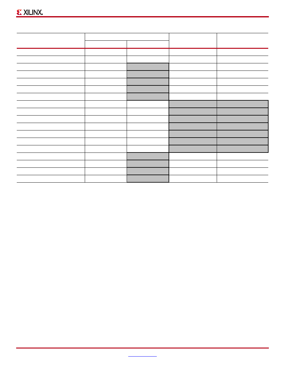
Table 8: Single-Ended I/O Standards
Signal Standard
(IOSTANDARD)
VCCO (Volts)
VREF for Inputs
(Volts)(1)
Board Termination
Voltage (VTT) in Volts
For Outputs
For Inputs
GTL
Note 2
0.8
1.2
GTLP
Note 2
11.5
HSTL_I
1.5
–
0.75
HSTL_III
1.5
–0.9
1.5
HSTL_I_18
1.8
–0.9
0.9
HSTL_II_18
1.8
–0.9
0.9
HSTL_III_18
1.8
–1.1
1.8
LVCMOS12
1.2
–
LVCMOS15
1.5
–
LVCMOS18
1.8
–
LVCMOS25
2.5
–
LVCMOS33
3.3
–
LVTTL
3.3
–
PCI33_3
3.0
–
SSTL18_I
1.8
–0.9
0.9
SSTL18_II
1.8
–0.9
0.9
SSTL2_I
2.5
–
1.25
SSTL2_II
2.5
–
1.25
Notes:
1.
Banks 4 and 5 of any Spartan-3 device in a VQ100 package do not support signal standards using VREF.
2.
The VCCO level used for the GTL and GTLP standards must be no lower than the termination voltage (VTT), nor can it be lower than the
voltage at the I/O pad.
3.
See Table 10 for a listing of the single-ended DCI standards.
相关PDF资料 |
PDF描述 |
|---|---|
| RSC36DTES | CONN EDGECARD 72POS .100 EYELET |
| ACB100DHRN | CONN CARD EXTEND 200POS .050" |
| XC3S2000-5FGG900C | SPARTAN-3A FPGA 2M 900-FBGA |
| ABB100DHRN | CONN CARD EXTEND 200POS .050" |
| ACB100DHRD | CONN CARD EXTEND 200POS .050" |
相关代理商/技术参数 |
参数描述 |
|---|---|
| XC3S2000-4FT256C | 制造商:XILINX 制造商全称:XILINX 功能描述:Spartan-3 FPGA |
| XC3S2000-4FT256I | 制造商:XILINX 制造商全称:XILINX 功能描述:Spartan-3 FPGA |
| XC3S2000-4PQ208C | 制造商:XILINX 制造商全称:XILINX 功能描述:Spartan-3 FPGA |
| XC3S2000-4PQ208I | 制造商:XILINX 制造商全称:XILINX 功能描述:Spartan-3 FPGA |
| XC3S2000-4PQG208C | 制造商:XILINX 制造商全称:XILINX 功能描述:Spartan-3 FPGA Family: Complete Data Sheet |
发布紧急采购,3分钟左右您将得到回复。