参数资料
| 型号: | XC3S5000-4FGG900I |
| 厂商: | Xilinx Inc |
| 文件页数: | 266/272页 |
| 文件大小: | 0K |
| 描述: | SPARTAN-3A FPGA 5M STD 900-FBGA |
| 产品培训模块: | Extended Spartan 3A FPGA Family |
| 标准包装: | 27 |
| 系列: | Spartan®-3 |
| LAB/CLB数: | 8320 |
| 逻辑元件/单元数: | 74880 |
| RAM 位总计: | 1916928 |
| 输入/输出数: | 633 |
| 门数: | 5000000 |
| 电源电压: | 1.14 V ~ 1.26 V |
| 安装类型: | 表面贴装 |
| 工作温度: | -40°C ~ 100°C |
| 封装/外壳: | 900-BBGA |
| 供应商设备封装: | 900-FBGA |
第1页第2页第3页第4页第5页第6页第7页第8页第9页第10页第11页第12页第13页第14页第15页第16页第17页第18页第19页第20页第21页第22页第23页第24页第25页第26页第27页第28页第29页第30页第31页第32页第33页第34页第35页第36页第37页第38页第39页第40页第41页第42页第43页第44页第45页第46页第47页第48页第49页第50页第51页第52页第53页第54页第55页第56页第57页第58页第59页第60页第61页第62页第63页第64页第65页第66页第67页第68页第69页第70页第71页第72页第73页第74页第75页第76页第77页第78页第79页第80页第81页第82页第83页第84页第85页第86页第87页第88页第89页第90页第91页第92页第93页第94页第95页第96页第97页第98页第99页第100页第101页第102页第103页第104页第105页第106页第107页第108页第109页第110页第111页第112页第113页第114页第115页第116页第117页第118页第119页第120页第121页第122页第123页第124页第125页第126页第127页第128页第129页第130页第131页第132页第133页第134页第135页第136页第137页第138页第139页第140页第141页第142页第143页第144页第145页第146页第147页第148页第149页第150页第151页第152页第153页第154页第155页第156页第157页第158页第159页第160页第161页第162页第163页第164页第165页第166页第167页第168页第169页第170页第171页第172页第173页第174页第175页第176页第177页第178页第179页第180页第181页第182页第183页第184页第185页第186页第187页第188页第189页第190页第191页第192页第193页第194页第195页第196页第197页第198页第199页第200页第201页第202页第203页第204页第205页第206页第207页第208页第209页第210页第211页第212页第213页第214页第215页第216页第217页第218页第219页第220页第221页第222页第223页第224页第225页第226页第227页第228页第229页第230页第231页第232页第233页第234页第235页第236页第237页第238页第239页第240页第241页第242页第243页第244页第245页第246页第247页第248页第249页第250页第251页第252页第253页第254页第255页第256页第257页第258页第259页第260页第261页第262页第263页第264页第265页当前第266页第267页第268页第269页第270页第271页第272页
Spartan-3 FPGA Family: DC and Switching Characteristics
DS099 (v3.1) June 27, 2013
Product Specification
93
Digital Clock Manager (DCM) Timing
For specification purposes, the DCM consists of three key components: the Delay-Locked Loop (DLL), the Digital Frequency
Synthesizer (DFS), and the Phase Shifter (PS).
Aspects of DLL operation play a role in all DCM applications. All such applications inevitably use the CLKIN and the CLKFB
inputs connected to either the CLK0 or the CLK2X feedback, respectively. Thus, specifications in the DLL tables (Table 58
and Table 59) apply to any application that only employs the DLL component. When the DFS and/or the PS components are
used together with the DLL, then the specifications listed in the DFS and PS tables (Table 60 through Table 63) supersede
any corresponding ones in the DLL tables. DLL specifications that do not change with the addition of DFS or PS functions
Period jitter and cycle-cycle jitter are two (of many) different ways of characterizing clock jitter. Both specifications describe
statistical variation from a mean value.
Period jitter is the worst-case deviation from the average clock period of all clock cycles in the collection of clock periods
sampled (usually from 100,000 to more than a million samples for specification purposes). In a histogram of period jitter, the
mean value is the clock period.
Cycle-cycle jitter is the worst-case difference in clock period between adjacent clock cycles in the collection of clock periods
sampled. In a histogram of cycle-cycle jitter, the mean value is zero.
Delay-Locked Loop (DLL)
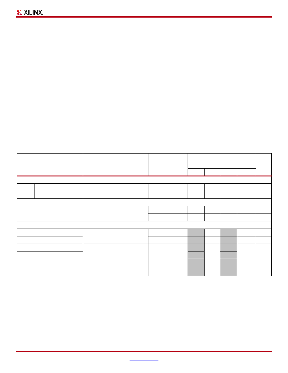
Table 58: Recommended Operating Conditions for the DLL
Symbol
Description
Frequency Mode/
FCLKIN Range
Speed Grade
Units
-5
-4
Min
Max
Min
Max
Input Frequency Ranges
FCLKIN
CLKIN_FREQ_DLL_LF
Frequency for the CLKIN input
Low
18(2)
167(3)
18(2)
167(3)
MHz
CLKIN_FREQ_DLL_HF
High
48
280(3)
48
280(3)(4)
MHz
Input Pulse Requirements
CLKIN_PULSE
CLKIN pulse width as a
percentage of the CLKIN period
FCLKIN ≤ 100 MHz
40%
60%
40%
60%
-
FCLKIN > 100 MHz
45%
55%
45%
55%
-
Input Clock Jitter Tolerance and Delay Path Variation(5)
CLKIN_CYC_JITT_DLL_LF
Cycle-to-cycle jitter at the CLKIN
input
Low
–
±300
–
±300
ps
CLKIN_CYC_JITT_DLL_HF
High
–
±150
–
±150
ps
CLKIN_PER_JITT_DLL_LF
Period jitter at the CLKIN input
All
–
±1
–
±1ns
CLKIN_PER_JITT_DLL_HF
–
CLKFB_DELAY_VAR_EXT
Allowable variation of off-chip
feedback delay from the DCM
output to the CLKFB input
All
–
±1
–
±1ns
Notes:
1.
DLL specifications apply when any of the DLL outputs (CLK0, CLK90, CLK180, CLK270, CLK2X, CLK2X180, or CLKDV) are in use.
2.
3.
The CLKIN_DIVIDE_BY_2 attribute can be used to increase the effective input frequency range up to FBUFG. When set to TRUE,
CLKIN_DIVIDE_BY_2 divides the incoming clock frequency by two as it enters the DCM.
4.
Industrial temperature range devices have additional requirements for continuous clocking, as specified in Table 64.
5.
CLKIN input jitter beyond these limits may cause the DCM to lose lock. See UG331 for more details.
相关PDF资料 |
PDF描述 |
|---|---|
| RSA50DTAZ-S273 | CONN EDGECARD 100PS R/A .125 SLD |
| 93LC86-I/P | IC EEPROM 16KBIT 3MHZ 8DIP |
| 93LC76/P | IC EEPROM 8KBIT 3MHZ 8DIP |
| XC6SLX100T-2FGG484I | IC FPGA SPARTAN 6 101K 484FGGBGA |
| RMA50DTAZ-S273 | CONN EDGECARD 100PS R/A .125 SLD |
相关代理商/技术参数 |
参数描述 |
|---|---|
| XC3S5000-5FG1156C | 制造商:Xilinx 功能描述: |
| XC3S5000-5FG676C | 制造商:Xilinx 功能描述:FPGA SPARTAN-3 5M GATES 74880 CELLS 725MHZ 1.2V 676FBGA - Trays |
| XC3S5000-5FG900C | 制造商:Xilinx 功能描述:FPGA SPARTAN-3 5M GATES 74880 CELLS 725MHZ 1.2V 900FBGA - Trays |
| XC3S5000-5FG900CES | 制造商:Xilinx 功能描述: |
| XC3S5000-5FGG676C | 功能描述:SPARTAN-3A FPGA 5M 676-FBGA RoHS:是 类别:集成电路 (IC) >> 嵌入式 - FPGA(现场可编程门阵列) 系列:Spartan®-3 产品变化通告:Step Intro and Pkg Change 11/March/2008 标准包装:1 系列:Virtex®-5 SXT LAB/CLB数:4080 逻辑元件/单元数:52224 RAM 位总计:4866048 输入/输出数:480 门数:- 电源电压:0.95 V ~ 1.05 V 安装类型:表面贴装 工作温度:-40°C ~ 100°C 封装/外壳:1136-BBGA,FCBGA 供应商设备封装:1136-FCBGA 配用:568-5088-ND - BOARD DEMO DAC1408D750122-1796-ND - EVALUATION PLATFORM VIRTEX-5 |
发布紧急采购,3分钟左右您将得到回复。