- 您现在的位置:买卖IC网 > PDF目录221636 > XC4005E-3TQG144C (XILINX INC) FPGA, 196 CLBS, 3000 GATES, 125 MHz, PQFP144 PDF资料下载
参数资料
| 型号: | XC4005E-3TQG144C |
| 厂商: | XILINX INC |
| 元件分类: | FPGA |
| 英文描述: | FPGA, 196 CLBS, 3000 GATES, 125 MHz, PQFP144 |
| 文件页数: | 14/17页 |
| 文件大小: | 75K |
| 代理商: | XC4005E-3TQG144C |
R
XC4000E and XC4000X Series Field Programmable Gate Arrays
6-106
February 11, 2000 (Version 1.8)
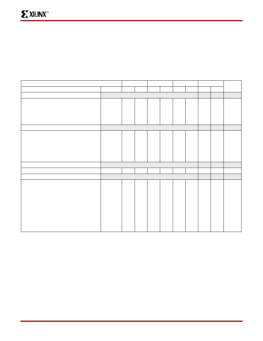
XC4000E CLB Characteristics Guidelines
Testing of switching parameters is modeled after testing methods specied by MIL-M-38510/605. All devices are 100%
functionally tested. Internal timing parameters are derived from measuring internal test patterns. Listed below are
representative values. For more specic, more precise, and worst-case guaranteed data, use the values reported by the
static timing analyzer (TRCE in the Xilinx Development System) and back-annotated to the simulation net list. These path
delays, provided as a guideline, have been extracted from the static timing analyzer report. All timing parameters assume
worst-case operating conditions (supply voltage and junction temperature). Values apply to all XC4000E devices unless
otherwise noted
CLB Switching Characteristics Guidelines
Speed Grade
-4
-3
-2
-1
Units
Description
Symbol
Min
Max
Min
Max
Min
Max
Min
Max
Combinatorial Delays
F/G inputs to X/Y outputs
F/G inputs via H to X/Y outputs
C inputs via SR through H to X/Y outputs
C inputs via H to X/Y outputs
C inputs via DIN through H to X/Y outputs
TILO
TIHO
THH0O
THH1O
THH2O
2.7
4.7
4.1
3.7
4.5
2.0
4.3
3.3
3.6
1.6
2.7
2.4
2.2
2.6
1.3
2.2
1.9
1.6
1.9
ns
CLB Fast Carry Logic
Operand inputs (F1, F2, G1, G4) to COUT
Add/Subtract input (F3) to COUT
Initialization inputs (F1, F3) to COUT
CIN through function generators to
X/Y outputs
CIN to COUT, bypass function generators
TOPCY
TASCY
TINCY
TSUM
TBYP
3.2
5.5
1.7
3.8
1.0
2.6
4.4
1.7
3.3
0.7
2.1
3.7
1.4
2.6
0.6
1.7
2.5
1.2
1.8
0.5
ns
Sequential Delays
Clock K to outputs Q
TCKO
3.7
2.8
1.9
ns
Setup Time before Clock K
F/G inputs
F/G inputs via H
C inputs via H0 through H
C inputs via H1 through H
C inputs via H2 through H
C inputs via DIN
C inputs via EC
C inputs via S/R, going Low (inactive)
CIN input via F/G
CIN input via F/G and H
TICK
TIHCK
THH0CK
THH1CK
THH2CK
TDICK
TECCK
TRCK
TCCK
TCHCK
4.0
6.1
4.5
5.0
4.8
3.0
4.0
4.2
2.5
4.2
3.0
4.6
3.6
4.1
3.8
2.4
3.0
4.0
2.1
3.5
2.4
3.9
3.5
3.3
3.7
2.0
2.6
4.0
1.8
2.8
2.4
2.1
2.5
1.0
2.0
1.5
ns
相关PDF资料 |
PDF描述 |
|---|---|
| XC4005E-3TQG144I | FPGA, 196 CLBS, 3000 GATES, 125 MHz, PQFP144 |
| XC4005E-4TQG144C | FPGA, 196 CLBS, 3000 GATES, 111 MHz, PQFP144 |
| XC4005E-4TQG144I | FPGA, 196 CLBS, 3000 GATES, 111 MHz, PQFP144 |
| XC4005E-1PQG100C | FPGA, 196 CLBS, 3000 GATES, 166 MHz, PQFP100 |
| XC4005E-2PQG100C | FPGA, 196 CLBS, 3000 GATES, 125 MHz, PQFP100 |
相关代理商/技术参数 |
参数描述 |
|---|---|
| XC4005E-4CB164B | 制造商:未知厂家 制造商全称:未知厂家 功能描述:Field Programmable Gate Array (FPGA) |
| XC4005E-4CB164M | 制造商:未知厂家 制造商全称:未知厂家 功能描述:Field Programmable Gate Array (FPGA) |
| XC4005E4PC84C | 制造商:XILINX 功能描述:New |
| XC4005E-4PC84C | 功能描述:IC FPGA 196 CLB'S 84-PLCC RoHS:否 类别:集成电路 (IC) >> 嵌入式 - FPGA(现场可编程门阵列) 系列:XC4000E/X 产品变化通告:XC4000(E,L) Discontinuation 01/April/2002 标准包装:24 系列:XC4000E/X LAB/CLB数:100 逻辑元件/单元数:238 RAM 位总计:3200 输入/输出数:80 门数:3000 电源电压:4.5 V ~ 5.5 V 安装类型:表面贴装 工作温度:-40°C ~ 100°C 封装/外壳:120-BCBGA 供应商设备封装:120-CPGA(34.55x34.55) |
| XC4005E-4PC84I | 制造商:未知厂家 制造商全称:未知厂家 功能描述:Field Programmable Gate Array (FPGA) |
发布紧急采购,3分钟左右您将得到回复。