- 您现在的位置:买卖IC网 > PDF目录221636 > XC4005E-3TQG144C (XILINX INC) FPGA, 196 CLBS, 3000 GATES, 125 MHz, PQFP144 PDF资料下载
参数资料
| 型号: | XC4005E-3TQG144C |
| 厂商: | XILINX INC |
| 元件分类: | FPGA |
| 英文描述: | FPGA, 196 CLBS, 3000 GATES, 125 MHz, PQFP144 |
| 文件页数: | 9/17页 |
| 文件大小: | 75K |
| 代理商: | XC4005E-3TQG144C |
R
February 11, 2000 (Version 1.8)
6-117
XC4000E and XC4000X Series Field Programmable Gate Arrays
6
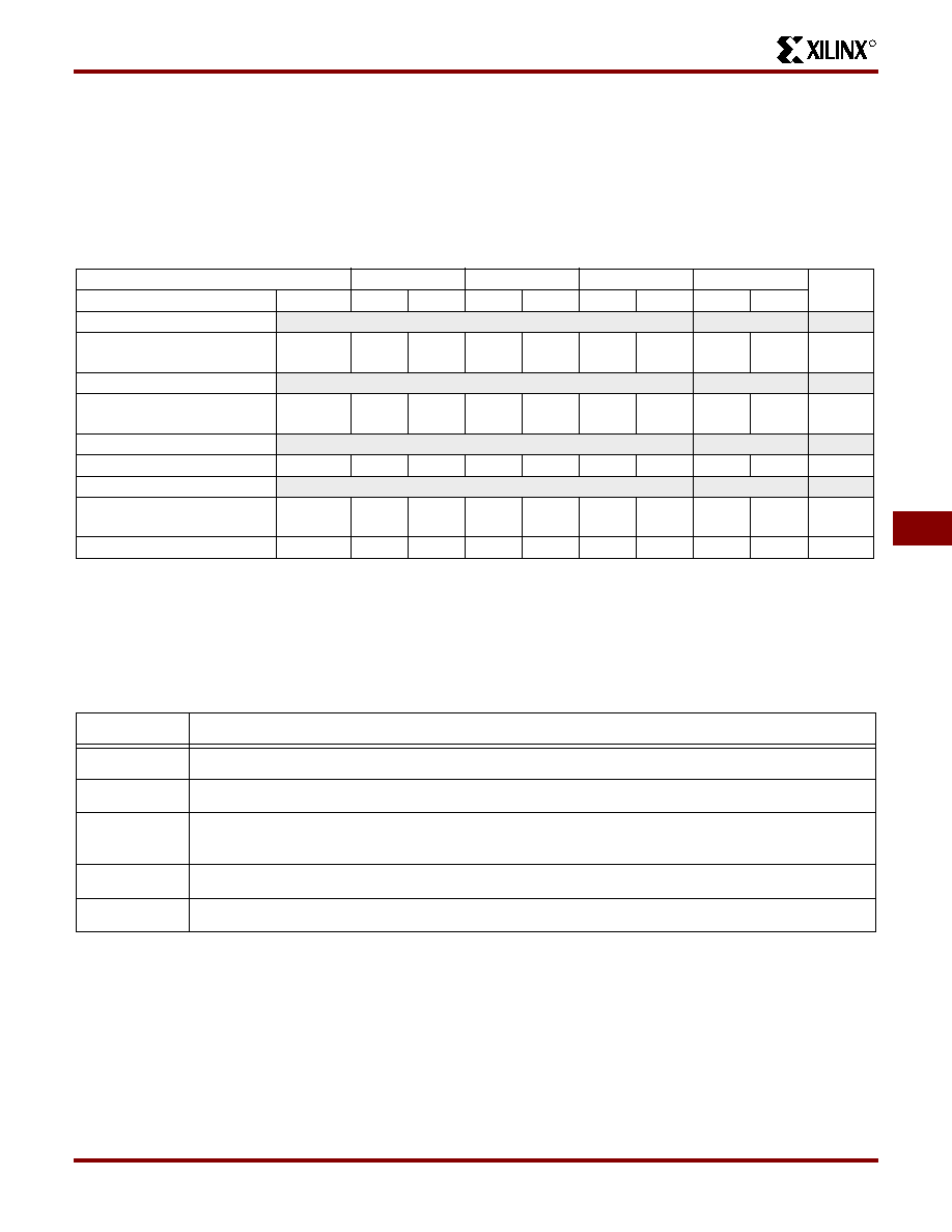
XC4000E Boundary Scan (JTAG) Switching Characteristic Guidelines
Testing of the switching parameters is modeled after testing methods specied by MIL-M-38510/605. All devices are 100%
functionally tested. Internal timing parameters are not measured directly. They are derived from benchmark timing patterns
that are taken at device introduction, prior to any process improvements. For more detailed, more precise, and more
up-to-date information, use the values provided by the XACT timing calculator and used in the simulator. These values can
be printed in tabular format by running LCA2XNF -S.
The following guidelines reect worst-case values over the recommended operating conditions. They are expressed in units
of nanoseconds and apply to all XC4000E devices unless otherwise noted.
Revision Control
Speed Grade
-4
-3
-2
-1
Units
Description
Symbol
Min
Max
Min
Max
Min
Max
Min
Max
Setup Times
Input (TDI) to clock (TCK)
Input (TMS) to clock (TCK)
TTDITCK
TTMSTCK
30.0
15.0
30.0
15.0
30.0
15.0
20.0
10.0
ns
Hold Times
Input (TDI) to clock (TCK)
Input (TMS) to clock (TCK)
TTCKTDI
TTCKTMS
0
ns
Propagation Delay
Clock (TCK) to Pad (TDO)
TTCKPO
30.0
20.0
ns
Clock
Clock (TCK) High
Clock (TCK) Low
TTCKH
TTCKL
5.0
4.0
ns
Frequency
FMAX
15.0
25.0
MHz
Note 1:
Input setup and hold times and clock-to-pad times are specied with respect to external signal pins.
Note 2:
Output timing is measured at pin threshold, with 50pF external capacitive loads (incl. test xture). Slew-rate limited output
rise/fall times are approximately two times longer than fast output rise/fall times. For the effect of capacitive loads on ground
bounce, see the “Additional XC4000 Data” section of the Programmable Logic Data Book.
Note 3:
Voltage levels of unused pads, bonded or unbonded, must be valid logic levels. Each can be congured with the internal
pull-up (default) or pull-down resistor, or congured as a driven output, or can be driven from an external source.
Version
Nature of Changes
3/30/98 (1.5)
As submitted for the 1999 data book
1/29/99 (1.5)
Updated Switching Characteristics Tables
5/14/99 (1.6)
Replaced Electrical Specification and pinout pages for E, EX, and XL families with separate updates
and added URL link on placeholder page for electrical specifications/pinouts for WebLINX users
8/27/99 (1.7)
Included missing IOB Propagation Delay page (6-113)
2/11/00 (1.8)
Altered IOB heads (Acrobat PDF file problem), corrected Dual-port Write Mins for -4 speed grade.
相关PDF资料 |
PDF描述 |
|---|---|
| XC4005E-3TQG144I | FPGA, 196 CLBS, 3000 GATES, 125 MHz, PQFP144 |
| XC4005E-4TQG144C | FPGA, 196 CLBS, 3000 GATES, 111 MHz, PQFP144 |
| XC4005E-4TQG144I | FPGA, 196 CLBS, 3000 GATES, 111 MHz, PQFP144 |
| XC4005E-1PQG100C | FPGA, 196 CLBS, 3000 GATES, 166 MHz, PQFP100 |
| XC4005E-2PQG100C | FPGA, 196 CLBS, 3000 GATES, 125 MHz, PQFP100 |
相关代理商/技术参数 |
参数描述 |
|---|---|
| XC4005E-4CB164B | 制造商:未知厂家 制造商全称:未知厂家 功能描述:Field Programmable Gate Array (FPGA) |
| XC4005E-4CB164M | 制造商:未知厂家 制造商全称:未知厂家 功能描述:Field Programmable Gate Array (FPGA) |
| XC4005E4PC84C | 制造商:XILINX 功能描述:New |
| XC4005E-4PC84C | 功能描述:IC FPGA 196 CLB'S 84-PLCC RoHS:否 类别:集成电路 (IC) >> 嵌入式 - FPGA(现场可编程门阵列) 系列:XC4000E/X 产品变化通告:XC4000(E,L) Discontinuation 01/April/2002 标准包装:24 系列:XC4000E/X LAB/CLB数:100 逻辑元件/单元数:238 RAM 位总计:3200 输入/输出数:80 门数:3000 电源电压:4.5 V ~ 5.5 V 安装类型:表面贴装 工作温度:-40°C ~ 100°C 封装/外壳:120-BCBGA 供应商设备封装:120-CPGA(34.55x34.55) |
| XC4005E-4PC84I | 制造商:未知厂家 制造商全称:未知厂家 功能描述:Field Programmable Gate Array (FPGA) |
发布紧急采购,3分钟左右您将得到回复。