- 您现在的位置:买卖IC网 > PDF目录300144 > XC4013E-1CB240M (Xilinx, Inc.) Programmable Gate Arrays PDF资料下载
参数资料
| 型号: | XC4013E-1CB240M |
| 厂商: | Xilinx, Inc. |
| 英文描述: | Programmable Gate Arrays |
| 中文描述: | 可编程门阵列 |
| 文件页数: | 58/68页 |
| 文件大小: | 462K |
| 代理商: | XC4013E-1CB240M |
第1页第2页第3页第4页第5页第6页第7页第8页第9页第10页第11页第12页第13页第14页第15页第16页第17页第18页第19页第20页第21页第22页第23页第24页第25页第26页第27页第28页第29页第30页第31页第32页第33页第34页第35页第36页第37页第38页第39页第40页第41页第42页第43页第44页第45页第46页第47页第48页第49页第50页第51页第52页第53页第54页第55页第56页第57页当前第58页第59页第60页第61页第62页第63页第64页第65页第66页第67页第68页
R
May 14, 1999 (Version 1.6)
6-65
XC4000E and XC4000X Series Field Programmable Gate Arrays
6
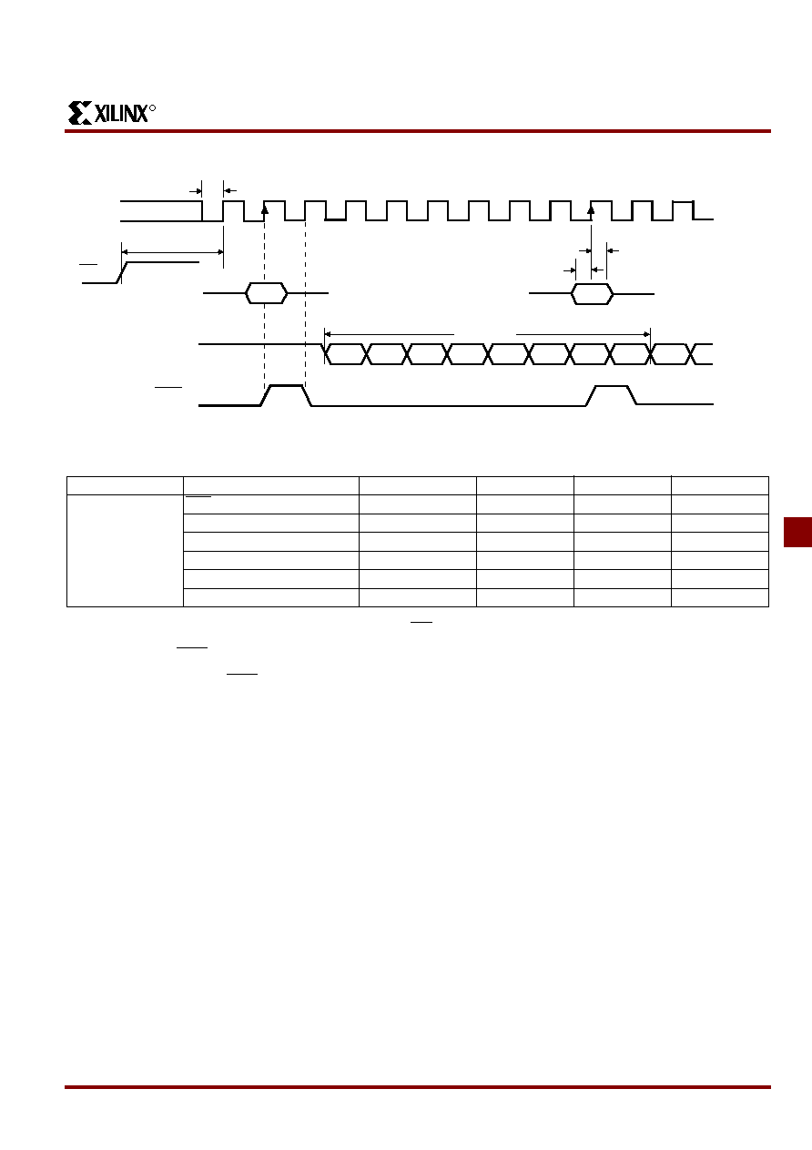
Figure 57: Synchronous Peripheral Mode Programming Switching Characteristics
0
DOUT
CCLK
1
2
345
6
7
BYTE
0
BYTE
1
BYTE 0 OUT
BYTE 1 OUT
RDY/BUSY
INIT
1
0
X6096
Description
Symbol
Min
Max
Units
CCLK
INIT (High) setup time
TIC
5
s
D0 - D7 setup time
TDC
60
ns
D0 - D7 hold time
TCD
0ns
CCLK High time
TCCH
50
ns
CCLK Low time
TCCL
60
ns
CCLK Frequency
FCC
8
MHz
Notes:
1. Peripheral Synchronous mode can be considered Slave Parallel mode. An external CCLK provides timing, clocking in the
rst data byte on the second rising edge of CCLK after INIT goes High. Subsequent data bytes are clocked in on every
eighth consecutive rising edge of CCLK.
2. The RDY/BUSY line goes High for one CCLK period after data has been clocked in, although synchronous operation does
not require such a response.
3. The pin name RDY/BUSY is a misnomer. In Synchronous Peripheral mode this is really an ACKNOWLEDGE signal.
4. Note that data starts to shift out serially on the DOUT pin 0.5 CCLK periods after it was loaded in parallel. Therefore,
additional CCLK pulses are clearly required after the last byte has been loaded.
相关PDF资料 |
PDF描述 |
|---|---|
| XC4013E-1HG240C | Programmable Gate Arrays |
| XC4013E-3BG240M | XC4000E and XC4000X Series Field Programmable Gate Arrays |
| XC4013E-1VQ240M | XC4000E and XC4000X Series Field Programmable Gate Arrays |
| XC4013E-2BG240C | XC4000E and XC4000X Series Field Programmable Gate Arrays |
| XC4013E-2BG240I | XC4000E and XC4000X Series Field Programmable Gate Arrays |
相关代理商/技术参数 |
参数描述 |
|---|---|
| XC4013E-1HG240C | 制造商:XILINX 制造商全称:XILINX 功能描述:Programmable Gate Arrays |
| XC4013E-1HG240I | 制造商:XILINX 制造商全称:XILINX 功能描述:Programmable Gate Arrays |
| XC4013E-1HG240M | 制造商:XILINX 制造商全称:XILINX 功能描述:Programmable Gate Arrays |
| XC4013E-1HQ208C | 功能描述:IC FPGA C-TEMP 5V 1SPD 208-HQFP RoHS:否 类别:集成电路 (IC) >> 嵌入式 - FPGA(现场可编程门阵列) 系列:XC4000E/X 标准包装:1 系列:Kintex-7 LAB/CLB数:25475 逻辑元件/单元数:326080 RAM 位总计:16404480 输入/输出数:350 门数:- 电源电压:0.97 V ~ 1.03 V 安装类型:表面贴装 工作温度:0°C ~ 85°C 封装/外壳:900-BBGA,FCBGA 供应商设备封装:900-FCBGA(31x31) 其它名称:122-1789 |
| XC4013E-1HQ208I | 制造商:未知厂家 制造商全称:未知厂家 功能描述:Field Programmable Gate Array (FPGA) |
发布紧急采购,3分钟左右您将得到回复。