- 您现在的位置:买卖IC网 > PDF目录300144 > XC4013E-1CB240M (Xilinx, Inc.) Programmable Gate Arrays PDF资料下载
参数资料
| 型号: | XC4013E-1CB240M |
| 厂商: | Xilinx, Inc. |
| 英文描述: | Programmable Gate Arrays |
| 中文描述: | 可编程门阵列 |
| 文件页数: | 68/68页 |
| 文件大小: | 462K |
| 代理商: | XC4013E-1CB240M |
第1页第2页第3页第4页第5页第6页第7页第8页第9页第10页第11页第12页第13页第14页第15页第16页第17页第18页第19页第20页第21页第22页第23页第24页第25页第26页第27页第28页第29页第30页第31页第32页第33页第34页第35页第36页第37页第38页第39页第40页第41页第42页第43页第44页第45页第46页第47页第48页第49页第50页第51页第52页第53页第54页第55页第56页第57页第58页第59页第60页第61页第62页第63页第64页第65页第66页第67页当前第68页
R
May 14, 1999 (Version 1.6)
6-13
XC4000E and XC4000X Series Field Programmable Gate Arrays
6
tions of the CLB, with the exception of the redenition of the
control signals. In 16x2 and 16x1 modes, the H’ function
generator can be used to implement Boolean functions of
F’, G’, and D1, and the D ip-ops can latch the F’, G’, H’, or
D0 signals.
Single-Port Edge-Triggered Mode
Edge-triggered
(synchronous)
RAM
simplies
timing
requirements. XC4000 Series edge-triggered RAM timing
operates like writing to a data register. Data and address
are presented. The register is enabled for writing by a logic
High on the write enable input, WE. Then a rising or falling
clock edge loads the data into the register, as shown in
Figure 3.
Complex timing relationships between address, data, and
write enable signals are not required, and the external write
enable pulse becomes a simple clock enable. The active
edge of WCLK latches the address, input data, and WE sig-
nals. An internal write pulse is generated that performs the
write. See Figure 4 and Figure 5 for block diagrams of a
CLB congured as 16x2 and 32x1 edge-triggered, sin-
gle-port RAM.
The relationships between CLB pins and RAM inputs and
outputs for single-port, edge-triggered mode are shown in
Table 5.
The Write Clock input (WCLK) can be congured as active
on either the rising edge (default) or the falling edge. It uses
the same CLB pin (K) used to clock the CLB ip-ops, but it
can be independently inverted. Consequently, the RAM
output can optionally be registered within the same CLB
either by the same clock edge as the RAM, or by the oppo-
site edge of this clock. The sense of WCLK applies to both
function generators in the CLB when both are congured
as RAM.
The WE pin is active-High and is not invertible within the
CLB.
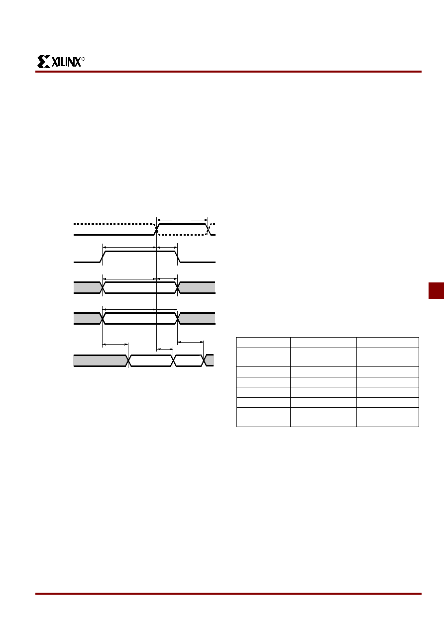
Note: The pulse following the active edge of WCLK (TWPS
in Figure 3) must be less than one millisecond wide. For
most applications, this requirement is not overly restrictive;
however, it must not be forgotten. Stopping WCLK at this
point in the write cycle could result in excessive current and
even damage to the larger devices if many CLBs are con-
gured as edge-triggered RAM.
X6461
WCLK (K)
WE
ADDRESS
DATA IN
DATA OUT
OLD
NEW
T
DSS
T
DHS
T
ASS
T
AHS
T
WSS
T
WPS
T
WHS
T
WOS
T
ILO
T
ILO
Figure 3:
Edge-Triggered RAM Write Timing
Table 5: Single-Port Edge-Triggered RAM Signals
RAM Signal
CLB Pin
Function
D
D0 or D1 (16x2,
16x1), D0 (32x1)
Data In
A[3:0]
F1-F4 or G1-G4
Address
A[4]
D1 (32x1)
Address
WE
Write Enable
WCLK
K
Clock
SPO
(Data Out)
F’ or G’
Single Port Out
(Data Out)
相关PDF资料 |
PDF描述 |
|---|---|
| XC4013E-1HG240C | Programmable Gate Arrays |
| XC4013E-3BG240M | XC4000E and XC4000X Series Field Programmable Gate Arrays |
| XC4013E-1VQ240M | XC4000E and XC4000X Series Field Programmable Gate Arrays |
| XC4013E-2BG240C | XC4000E and XC4000X Series Field Programmable Gate Arrays |
| XC4013E-2BG240I | XC4000E and XC4000X Series Field Programmable Gate Arrays |
相关代理商/技术参数 |
参数描述 |
|---|---|
| XC4013E-1HG240C | 制造商:XILINX 制造商全称:XILINX 功能描述:Programmable Gate Arrays |
| XC4013E-1HG240I | 制造商:XILINX 制造商全称:XILINX 功能描述:Programmable Gate Arrays |
| XC4013E-1HG240M | 制造商:XILINX 制造商全称:XILINX 功能描述:Programmable Gate Arrays |
| XC4013E-1HQ208C | 功能描述:IC FPGA C-TEMP 5V 1SPD 208-HQFP RoHS:否 类别:集成电路 (IC) >> 嵌入式 - FPGA(现场可编程门阵列) 系列:XC4000E/X 标准包装:1 系列:Kintex-7 LAB/CLB数:25475 逻辑元件/单元数:326080 RAM 位总计:16404480 输入/输出数:350 门数:- 电源电压:0.97 V ~ 1.03 V 安装类型:表面贴装 工作温度:0°C ~ 85°C 封装/外壳:900-BBGA,FCBGA 供应商设备封装:900-FCBGA(31x31) 其它名称:122-1789 |
| XC4013E-1HQ208I | 制造商:未知厂家 制造商全称:未知厂家 功能描述:Field Programmable Gate Array (FPGA) |
发布紧急采购,3分钟左右您将得到回复。