- 您现在的位置:买卖IC网 > PDF目录300144 > XC4013E-1HG240C (Xilinx, Inc.) Programmable Gate Arrays PDF资料下载
参数资料
| 型号: | XC4013E-1HG240C |
| 厂商: | Xilinx, Inc. |
| 英文描述: | Programmable Gate Arrays |
| 中文描述: | 可编程门阵列 |
| 文件页数: | 56/68页 |
| 文件大小: | 462K |
| 代理商: | XC4013E-1HG240C |
第1页第2页第3页第4页第5页第6页第7页第8页第9页第10页第11页第12页第13页第14页第15页第16页第17页第18页第19页第20页第21页第22页第23页第24页第25页第26页第27页第28页第29页第30页第31页第32页第33页第34页第35页第36页第37页第38页第39页第40页第41页第42页第43页第44页第45页第46页第47页第48页第49页第50页第51页第52页第53页第54页第55页当前第56页第57页第58页第59页第60页第61页第62页第63页第64页第65页第66页第67页第68页
R
XC4000E and XC4000X Series Field Programmable Gate Arrays
6-10
May 14, 1999 (Version 1.6)
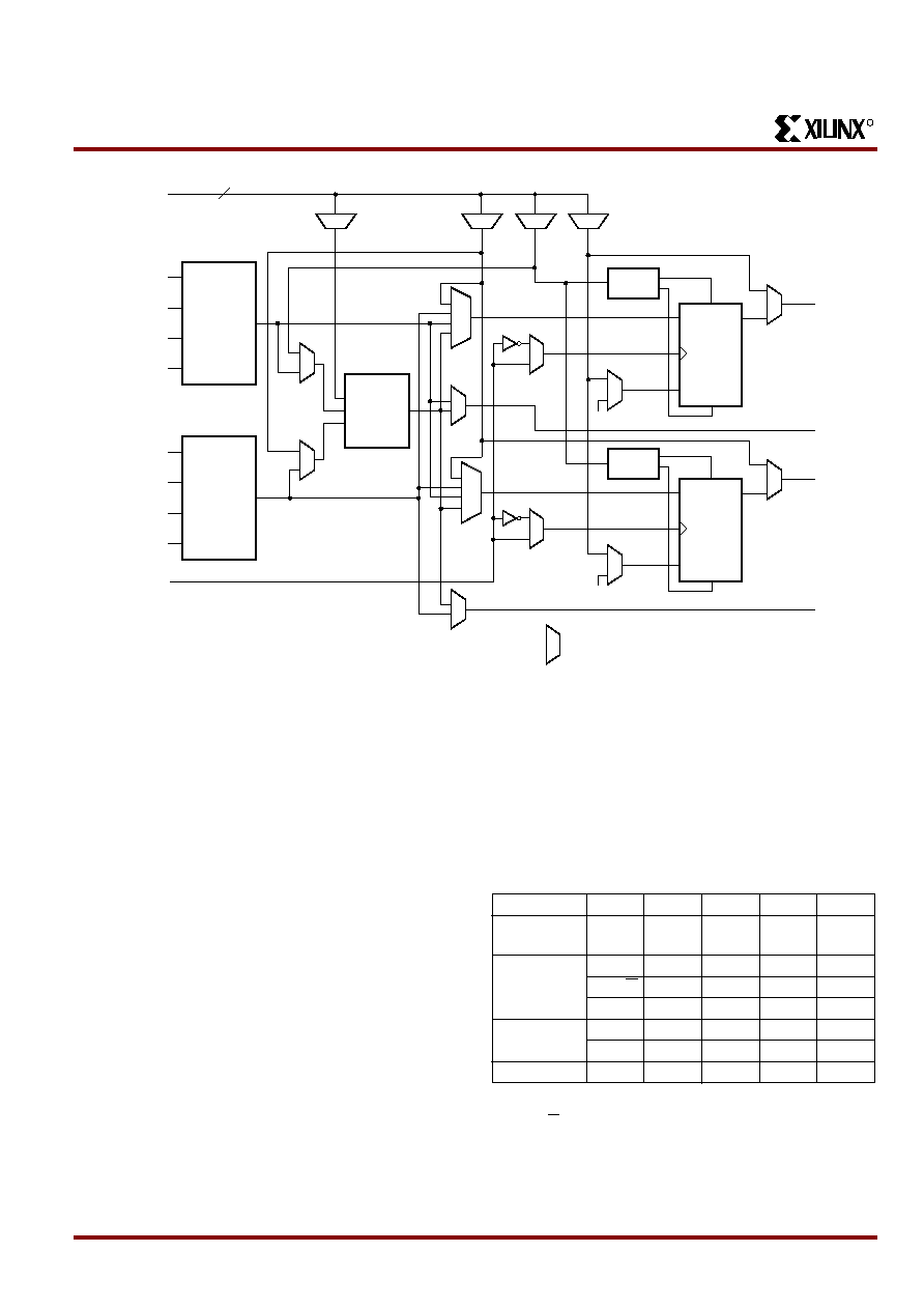
Flip-Flops
The CLB can pass the combinatorial output(s) to the inter-
connect network, but can also store the combinatorial
results or other incoming data in one or two ip-ops, and
connect their outputs to the interconnect network as well.
The two edge-triggered D-type ip-ops have common
clock (K) and clock enable (EC) inputs. Either or both clock
inputs can also be permanently enabled. Storage element
functionality is described in Table 2.
Latches (XC4000X only)
The CLB storage elements can also be congured as
latches. The two latches have common clock (K) and clock
enable (EC) inputs. Storage element functionality is
described in Table 2.
Clock Input
Each ip-op can be triggered on either the rising or falling
clock edge. The clock pin is shared by both storage ele-
ments. However, the clock is individually invertible for each
storage element. Any inverter placed on the clock input is
automatically absorbed into the CLB.
Clock Enable
The clock enable signal (EC) is active High. The EC pin is
shared by both storage elements. If left unconnected for
either, the clock enable for that storage element defaults to
the active state. EC is not invertible within the CLB.
LOGIC
FUNCTION
OF
G1-G4
G4
G3
G2
G1
G'
LOGIC
FUNCTION
OF
F1-F4
F4
F3
F2
F1
F'
LOGIC
FUNCTION
OF
F', G',
AND
H1
H'
DIN
F'
G'
H'
DIN
F'
G'
H'
G'
H'
F'
S/R
CONTROL
D
EC
RD
Bypass
SD
YQ
XQ
Q
S/R
CONTROL
D
EC
RD
SD
Q
1
K
(CLOCK)
Multiplexer Controlled
by Configuration Program
Y
X
DIN/H2
H1
SR/H0
EC
X6692
C1 C4
4
Figure 1: Simplied Block Diagram of XC4000 Series CLB (RAM and Carry Logic functions not shown)
Table 2: CLB Storage Element Functionality
(active rising edge is shown)
Mode
K
EC
SR
D
Q
Power-Up or
GSR
XXXX
SR
Flip-Flop
XX
1
X
SR
__/
1*
0*
D
0X
0*
X
Q
Latch
11*
0*
X
Q
01*
0*
D
Both
X
0
0*
X
Q
Legend:
X
__/
SR
0*
1*
Don’t care
Rising edge
Set or Reset value. Reset is default.
Input is Low or unconnected (default value)
Input is High or unconnected (default value)
相关PDF资料 |
PDF描述 |
|---|---|
| XC4013E-3BG240M | XC4000E and XC4000X Series Field Programmable Gate Arrays |
| XC4013E-1VQ240M | XC4000E and XC4000X Series Field Programmable Gate Arrays |
| XC4013E-2BG240C | XC4000E and XC4000X Series Field Programmable Gate Arrays |
| XC4013E-2BG240I | XC4000E and XC4000X Series Field Programmable Gate Arrays |
| XC4013E-2BG240M | XC4000E and XC4000X Series Field Programmable Gate Arrays |
相关代理商/技术参数 |
参数描述 |
|---|---|
| XC4013E-1HG240I | 制造商:XILINX 制造商全称:XILINX 功能描述:Programmable Gate Arrays |
| XC4013E-1HG240M | 制造商:XILINX 制造商全称:XILINX 功能描述:Programmable Gate Arrays |
| XC4013E-1HQ208C | 功能描述:IC FPGA C-TEMP 5V 1SPD 208-HQFP RoHS:否 类别:集成电路 (IC) >> 嵌入式 - FPGA(现场可编程门阵列) 系列:XC4000E/X 标准包装:1 系列:Kintex-7 LAB/CLB数:25475 逻辑元件/单元数:326080 RAM 位总计:16404480 输入/输出数:350 门数:- 电源电压:0.97 V ~ 1.03 V 安装类型:表面贴装 工作温度:0°C ~ 85°C 封装/外壳:900-BBGA,FCBGA 供应商设备封装:900-FCBGA(31x31) 其它名称:122-1789 |
| XC4013E-1HQ208I | 制造商:未知厂家 制造商全称:未知厂家 功能描述:Field Programmable Gate Array (FPGA) |
| XC4013E-1HQ240C | 功能描述:IC FPGA C-TEMP 5V 1SPD 240-HQFP RoHS:否 类别:集成电路 (IC) >> 嵌入式 - FPGA(现场可编程门阵列) 系列:XC4000E/X 标准包装:1 系列:Kintex-7 LAB/CLB数:25475 逻辑元件/单元数:326080 RAM 位总计:16404480 输入/输出数:350 门数:- 电源电压:0.97 V ~ 1.03 V 安装类型:表面贴装 工作温度:0°C ~ 85°C 封装/外壳:900-BBGA,FCBGA 供应商设备封装:900-FCBGA(31x31) 其它名称:122-1789 |
发布紧急采购,3分钟左右您将得到回复。