- 您现在的位置:买卖IC网 > PDF目录277724 > XC4013E-2BGG225I (XILINX INC) FPGA, 576 CLBS, 10000 GATES, 125 MHz, PBGA225 PDF资料下载
参数资料
| 型号: | XC4013E-2BGG225I |
| 厂商: | XILINX INC |
| 元件分类: | FPGA |
| 英文描述: | FPGA, 576 CLBS, 10000 GATES, 125 MHz, PBGA225 |
| 文件页数: | 2/17页 |
| 文件大小: | 75K |
| 代理商: | XC4013E-2BGG225I |
R
XC4000E and XC4000X Series Field Programmable Gate Arrays
6-110
February 11, 2000 (Version 1.8)
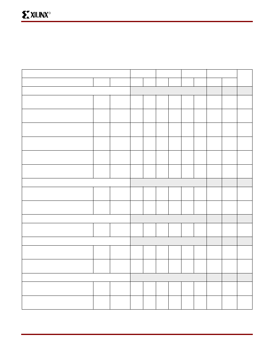
CLB Level-Sensitive RAM Switching Characteristic Guidelines
Testing of switching parameters is modeled after testing methods specied by MIL-M-38510/605. All devices are 100%
functionally tested. Internal timing parameters are derived from measuring internal test patterns. Listed below are
representative values. For more specic, more precise, and worst-case guaranteed data, use the values reported by the
static timing analyzer (TRCE in the Xilinx Development System) and back-annotated to the simulation net list. All timing
parameters assume worst-case operating conditions (supply voltage and junction temperature). Values apply to all
XC4000E devices unless otherwise noted.
Speed Grade
-4
-3
-2
-1
Units
Description
Size
Symbol
Min
Max
Min
Max
Min
Max
Min
Max
Write Operation
Address write cycle time
16x2
32x1
TWC
TWCT
8.0
ns
Write Enable pulse width (High)
16x2
32x1
TWP
TWPT
4.0
ns
Address setup time before WE
16x2
32x1
TAS
TAST
2.0
ns
Address hold time after end of WE
16x2
32x1
TAH
TAHT
2.5
2.0
ns
DIN setup time before end of WE
16x2
32x1
TDS
TDST
4.0
5.0
2.2
0.8
ns
DIN hold time after end of WE
16x2
32x1
TDH
TDHT
2.0
ns
Read Operation
Address read cycle time
16x2
32x1
TRC
TRCT
4.5
6.5
3.1
5.5
2.6
3.8
2.6
3.8
ns
Data valid after address change
(no Write Enable)
16x2
32x1
TILO
TIHO
2.7
4.7
1.8
3.2
1.6
2.7
1.6
2.7
ns
Read Operation, Clocking Data into Flip-Flop
Address setup time before clock K
16x2
32x1
TICK
TIHCK
4.0
6.1
3.0
4.6
2.4
3.9
2.4
3.9
ns
Read During Write
Data valid after WE goes active (DIN
stable before WE)
16x2
32x1
TWO
TWOT
10.0
12.0
6.0
7.3
4.9
5.6
4.9
5.6
ns
Data valid after DIN
(DIN changes during WE)
16x2
32x1
TDO
TDOT
9.0
11.0
6.6
7.6
5.8
6.2
5.8
6.2
ns
Read During Write, Clocking Data into Flip-Flop
WE setup time before clock K
16x2
32x1
TWCK
TWCKT
8.0
9.6
6.0
6.8
5.1
5.8
5.1
5.8
ns
Data setup time before clock K
16x2
32x1
TDCK
TDCKT
7.0
8.0
5.2
6.2
4.4
5.3
4.4
5.3
ns
Note 1: Timing for the 16x1 RAM option is identical to 16x2 RAM timing.
相关PDF资料 |
PDF描述 |
|---|---|
| XC4013E-3HQG240C | FPGA, 576 CLBS, 10000 GATES, 125 MHz, PQFP240 |
| XC4013E-3HQG240I | FPGA, 576 CLBS, 10000 GATES, 125 MHz, PQFP240 |
| XC4013E-4HQG240C | FPGA, 576 CLBS, 10000 GATES, 111 MHz, PQFP240 |
| XC4013E-4HQG240I | FPGA, 576 CLBS, 10000 GATES, 111 MHz, PQFP240 |
| XC4013E-3HQG208C | FPGA, 576 CLBS, 10000 GATES, 125 MHz, PQFP208 |
相关代理商/技术参数 |
参数描述 |
|---|---|
| XC4013E-2CB240C | 制造商:XILINX 制造商全称:XILINX 功能描述:Programmable Gate Arrays |
| XC4013E-2CB240I | 制造商:XILINX 制造商全称:XILINX 功能描述:Programmable Gate Arrays |
| XC4013E-2CB240M | 制造商:XILINX 制造商全称:XILINX 功能描述:Programmable Gate Arrays |
| XC4013E-2HG240C | 制造商:XILINX 制造商全称:XILINX 功能描述:Programmable Gate Arrays |
| XC4013E-2HG240I | 制造商:XILINX 制造商全称:XILINX 功能描述:Programmable Gate Arrays |
发布紧急采购,3分钟左右您将得到回复。