参数资料
| 型号: | XC4025E-3HQ240C |
| 厂商: | Xilinx Inc |
| 文件页数: | 3/68页 |
| 文件大小: | 0K |
| 描述: | IC FPGA 1024 CLB'S 240-HQFP |
| 产品变化通告: | XC4000(XL,XLA,E) Discontinuation 15/Nov/2004 |
| 标准包装: | 24 |
| 系列: | XC4000E/X |
| LAB/CLB数: | 1024 |
| 逻辑元件/单元数: | 2432 |
| RAM 位总计: | 32768 |
| 输入/输出数: | 193 |
| 门数: | 25000 |
| 电源电压: | 4.75 V ~ 5.25 V |
| 安装类型: | 表面贴装 |
| 工作温度: | 0°C ~ 85°C |
| 封装/外壳: | 240-BFQFP 裸露焊盘 |
| 供应商设备封装: | 240-PQFP(32x32) |
| 其它名称: | 122-1119 |
第1页第2页当前第3页第4页第5页第6页第7页第8页第9页第10页第11页第12页第13页第14页第15页第16页第17页第18页第19页第20页第21页第22页第23页第24页第25页第26页第27页第28页第29页第30页第31页第32页第33页第34页第35页第36页第37页第38页第39页第40页第41页第42页第43页第44页第45页第46页第47页第48页第49页第50页第51页第52页第53页第54页第55页第56页第57页第58页第59页第60页第61页第62页第63页第64页第65页第66页第67页第68页
R
May 14, 1999 (Version 1.6)
6-15
XC4000E and XC4000X Series Field Programmable Gate Arrays
6
Dual-Port Edge-Triggered Mode
In dual-port mode, both the F and G function generators
are used to create a single 16x1 RAM array with one write
port and two read ports. The resulting RAM array can be
read and written simultaneously at two independent
addresses. Simultaneous read and write operations at the
same address are also supported.
Dual-port mode always has edge-triggered write timing, as
shown in Figure 3.
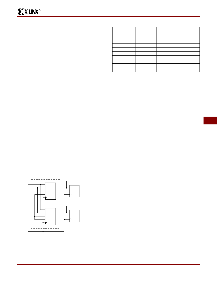
Figure 6 shows a simple model of an XC4000 Series CLB
congured as dual-port RAM. One address port, labeled
A[3:0], supplies both the read and write address for the F
function generator. This function generator behaves the
same as a 16x1 single-port edge-triggered RAM array. The
RAM output, Single Port Out (SPO), appears at the F func-
tion generator output. SPO, therefore, reects the data at
address A[3:0].
The other address port, labeled DPRA[3:0] for Dual Port
Read Address, supplies the read address for the G function
generator. The write address for the G function generator,
however, comes from the address A[3:0]. The output from
this 16x1 RAM array, Dual Port Out (DPO), appears at the
G function generator output. DPO, therefore, reects the
data at address DPRA[3:0].
Therefore, by using A[3:0] for the write address and
DPRA[3:0] for the read address, and reading only the DPO
output, a FIFO that can read and write simultaneously is
easily generated. Simultaneous access doubles the effec-
tive throughput of the FIFO.
The relationships between CLB pins and RAM inputs and
outputs for dual-port, edge-triggered mode are shown in
Table 6. See Figure 7 on page 16 for a block diagram of a
CLB congured in this mode.
Table 6: Dual-Port Edge-Triggered RAM Signals
Note: The pulse following the active edge of WCLK (TWPS
in Figure 3) must be less than one millisecond wide. For
most applications, this requirement is not overly restrictive;
however, it must not be forgotten. Stopping WCLK at this
point in the write cycle could result in excessive current and
even damage to the larger devices if many CLBs are con-
gured as edge-triggered RAM.
Single-Port Level-Sensitive Timing Mode
Note: Edge-triggered mode is recommended for all new
designs. Level-sensitive mode, also called asynchronous
mode, is still supported for XC4000 Series backward-com-
patibility with the XC4000 family.
Level-sensitive RAM timing is simple in concept but can be
complicated in execution. Data and address signals are
presented, then a positive pulse on the write enable pin
(WE) performs a write into the RAM at the designated
address. As indicated by the “level-sensitive” label, this
RAM acts like a latch. During the WE High pulse, changing
the data lines results in new data written to the old address.
Changing the address lines while WE is High results in spu-
rious data written to the new address—and possibly at
other addresses as well, as the address lines inevitably do
not all change simultaneously.
The user must generate a carefully timed WE signal. The
delay on the WE signal and the address lines must be care-
fully veried to ensure that WE does not become active
until after the address lines have settled, and that WE goes
inactive before the address lines change again. The data
must be stable before and after the falling edge of WE.
In practical terms, WE is usually generated by a 2X clock. If
a 2X clock is not available, the falling edge of the system
clock can be used. However, there are inherent risks in this
approach, since the WE pulse must be guaranteed inactive
before the next rising edge of the system clock. Several
older application notes are available from Xilinx that dis-
cuss the design of level-sensitive RAMs.
However, the edge-triggered RAM available in the XC4000
Series is superior to level-sensitive RAM for almost every
application.
WE
DD
Q
DQ
D
DPRA[3:0]
A[3:0]
AR[3:0]
AW[3:0]
WE
D
AR[3:0]
AW[3:0]
RAM16X1D Primitive
F Function Generator
G Function Generator
DPO (Dual Port Out)
Registered DPO
SPO (Single Port Out)
Registered SPO
WCLK
X6755
Figure 6: XC4000 Series Dual-Port RAM, Simple
Model
RAM Signal
CLB Pin
Function
D
D0
Data In
A[3:0]
F1-F4
Read Address for F,
Write Address for F and G
DPRA[3:0]
G1-G4
Read Address for G
WE
Write Enable
WCLK
K
Clock
SPO
F’
Single Port Out
(addressed by A[3:0])
DPO
G’
Dual Port Out
(addressed by DPRA[3:0])
Product Obsolete or Under Obsolescence
相关PDF资料 |
PDF描述 |
|---|---|
| XC4013E-3PQ160C | IC FPGA 576 CLB'S 160-PQFP |
| XC4010E-4PQ208C | IC FPGA 400 CLB'S 208-PQFP |
| A1225A-1PQG100I | IC FPGA 2500 GATES 100-PQFP IND |
| IDT71V416L15BEGI8 | IC SRAM 4MBIT 15NS 48FBGA |
| XC4025E-2HQ240C | IC FPGA 1024 CLB'S 240-HQFP |
相关代理商/技术参数 |
参数描述 |
|---|---|
| XC4025E-3HQ240I | 功能描述:IC FPGA I-TEMP 5V 3SPD 240-PQFP RoHS:否 类别:集成电路 (IC) >> 嵌入式 - FPGA(现场可编程门阵列) 系列:XC4000E/X 标准包装:1 系列:Kintex-7 LAB/CLB数:25475 逻辑元件/单元数:326080 RAM 位总计:16404480 输入/输出数:350 门数:- 电源电压:0.97 V ~ 1.03 V 安装类型:表面贴装 工作温度:0°C ~ 85°C 封装/外壳:900-BBGA,FCBGA 供应商设备封装:900-FCBGA(31x31) 其它名称:122-1789 |
| XC4025E-3HQ304C | 功能描述:IC FPGA C-TEMP 5V 3SPD 304-HQFP RoHS:否 类别:集成电路 (IC) >> 嵌入式 - FPGA(现场可编程门阵列) 系列:XC4000E/X 标准包装:1 系列:Kintex-7 LAB/CLB数:25475 逻辑元件/单元数:326080 RAM 位总计:16404480 输入/输出数:350 门数:- 电源电压:0.97 V ~ 1.03 V 安装类型:表面贴装 工作温度:0°C ~ 85°C 封装/外壳:900-BBGA,FCBGA 供应商设备封装:900-FCBGA(31x31) 其它名称:122-1789 |
| XC4025E3HQ304I | 制造商:XILINX 功能描述:New |
| XC4025E-3HQ304I | 功能描述:IC FPGA I-TEMP 5V 3SPD 304-HQFP RoHS:否 类别:集成电路 (IC) >> 嵌入式 - FPGA(现场可编程门阵列) 系列:XC4000E/X 标准包装:1 系列:Kintex-7 LAB/CLB数:25475 逻辑元件/单元数:326080 RAM 位总计:16404480 输入/输出数:350 门数:- 电源电压:0.97 V ~ 1.03 V 安装类型:表面贴装 工作温度:0°C ~ 85°C 封装/外壳:900-BBGA,FCBGA 供应商设备封装:900-FCBGA(31x31) 其它名称:122-1789 |
| XC4025E-3PG223C | 功能描述:IC FPGA C-TEMP 5V 3SPD 223-CPGA RoHS:否 类别:集成电路 (IC) >> 嵌入式 - FPGA(现场可编程门阵列) 系列:XC4000E/X 标准包装:1 系列:Kintex-7 LAB/CLB数:25475 逻辑元件/单元数:326080 RAM 位总计:16404480 输入/输出数:350 门数:- 电源电压:0.97 V ~ 1.03 V 安装类型:表面贴装 工作温度:0°C ~ 85°C 封装/外壳:900-BBGA,FCBGA 供应商设备封装:900-FCBGA(31x31) 其它名称:122-1789 |
发布紧急采购,3分钟左右您将得到回复。