参数资料
| 型号: | XC4028XL-09HQ208C |
| 厂商: | Xilinx Inc |
| 文件页数: | 15/16页 |
| 文件大小: | 0K |
| 描述: | IC FPGA C-TEMP 3.3V 208-HQFP |
| 产品变化通告: | Product Discontinuation 19/Feb/2007 |
| 标准包装: | 1 |
| 系列: | XC4000E/X |
| LAB/CLB数: | 1024 |
| 逻辑元件/单元数: | 2432 |
| RAM 位总计: | 32768 |
| 输入/输出数: | 160 |
| 门数: | 28000 |
| 电源电压: | 3 V ~ 3.6 V |
| 安装类型: | 表面贴装 |
| 工作温度: | 0°C ~ 85°C |
| 封装/外壳: | 208-BFQFP 裸露焊盘 |
| 供应商设备封装: | 208-PQFP(28x28) |
R
XC4000E and XC4000X Series Field Programmable Gate Arrays
6-80
DS005 (v2.0) March 1, 2013 - Product Specification
Product Obsolete/Under Obsolescence
XC4000XL Pin-to-Pin Output Parameter Guidelines
Testing of switching parameters is modeled after testing methods specified by MIL-M-38510/605. All devices are 100%
functionally tested. Pin-to-pin timing parameters are derived from measuring external and internal test patterns and are
guaranteed over worst-case operating conditions (supply voltage and junction temperature). Listed below are representative
values for typical pin locations and normal clock loading. For more specific, more precise, and worst-case guaranteed data,
reflecting the actual routing structure, use the values provided by the static timing analyzer (TRCE in the Xilinx Development
System) and back-annotated to the simulation netlist. These path delays, provided as a guideline, have been extracted from
the static timing analyzer report. Values are expressed in nanoseconds unless otherwise noted.
Output Flip-Flop, Clock to Out
Capacitive Load Factor
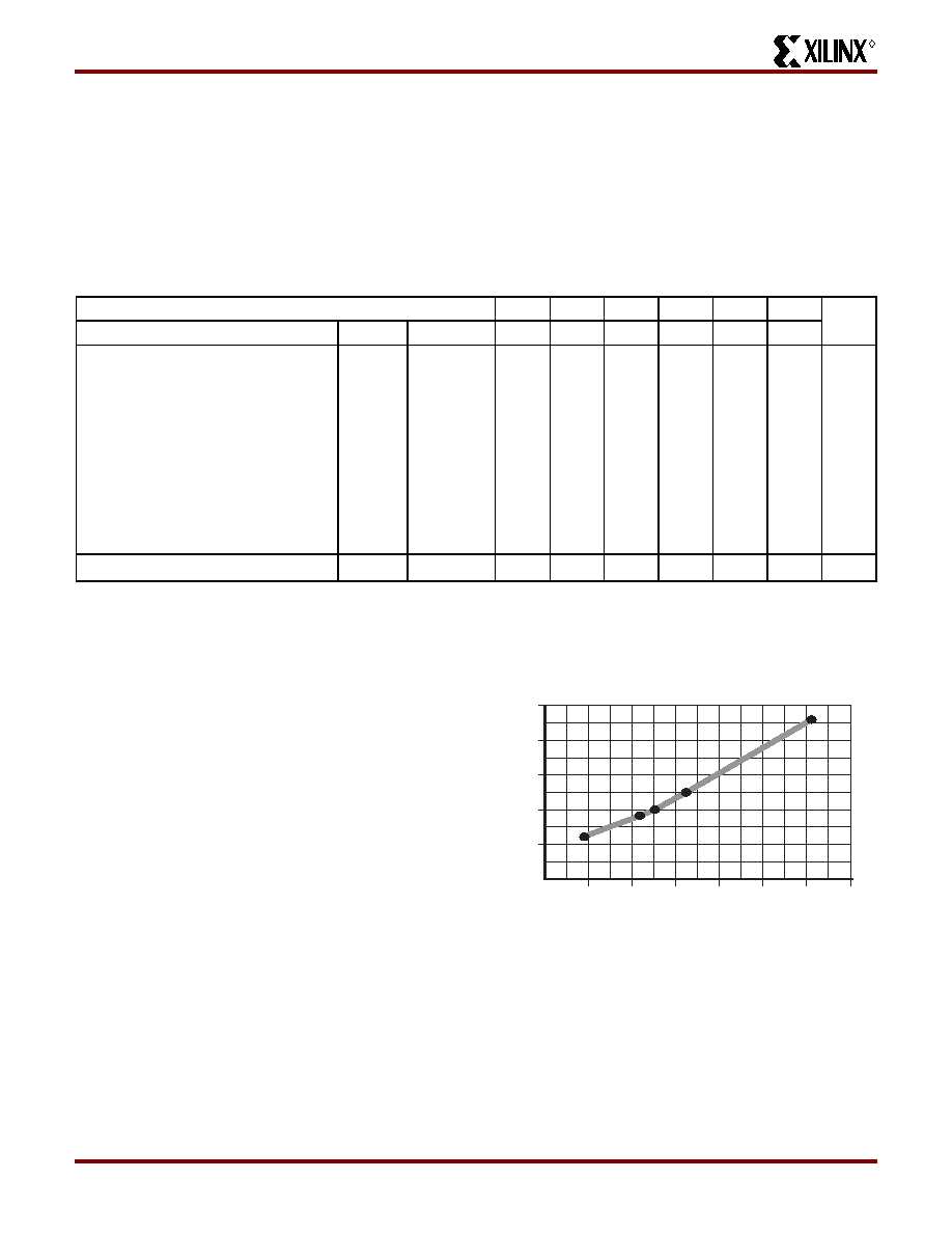
Figure 1 shows the relationship between I/O output delay
and load capacitance. It allows a user to adjust the speci-
fied output delay if the load capacitance is different than
50 pF. For example, if the actual load capacitance is
120 pF, add 2.5 ns to the specified delay. If the load capac-
itance is 20 pF, subtract 0.8 ns from the specified output
delay.
Figure 1 is usable over the specified operating conditions of
voltage and temperature and is independent of the output
slew rate control.
Figure 1: Delay Factor at Various Capacitive Loads
Speed Grade
All
-3
-2
-1
-09
-08
Units
Description
Symbol
Device
Min
Max
Global Low Skew Clock to Output us-
ing Output Flip Flop
TICKOF
XC4002XL
XC4005XL
XC4010XL
XC4013XL
XC4020XL
XC4028XL
XC4036XL
XC4044XL
XC4052XL
XC4062XL
XC4085XL
1.2
1.3
1.4
1.5
1.6
1.8
2.0
2.1
2.2
2.3
2.5
7.1
7.7
8.2
8.6
9.0
9.4
9.8
10.3
10.7
11.3
12.2
6.1
6.6
7.1
7.4
7.8
8.1
8.5
8.9
9.3
9.7
10.5
5.4
5.8
6.2
6.5
6.8
7.1
7.4
7.8
8.3
8.5
9.5
5.1
5.4
5.8
6.1
6.4
6.7
7.0
7.4
7.9
8.1
9.0
5.6
6.4
7.3
ns
For output SLOW option add
TSLOW
All Devices
0.5
3.0
2.5
2.0
1.7
1.6
ns
Notes:
Clock-to-out minimum delay is measured with the fastest route and the lightest load, Clock-to-out maximum delay is
measured using the farthest distance and a reference load of one clock pin (IK or OK) per IOB as well as driving all
accessible CLB flip-flops. For designs with a smaller number of clock loads, the pad-to-IOB clock pin delay as determined
by the static timing analyzer (TRCE) can be added to the AC parameter Tokpof and used as a worst-case pin-to-pin
clock-to-out delay for clocked outputs for FAST mode configurations.
Output timing is measured at ~50% VCC threshold with 50 pF external capacitive load. For different loads, see Figure 1.
X8257
-2
0
20
406080
Capacitance (pF)
Delta
Dela
y
(ns)
100
120
140
-1
0
1
2
3
相关PDF资料 |
PDF描述 |
|---|---|
| XC4028XL-09BG352C | IC FPGA C-TEMP 3.3V 352-MBGA |
| MPC8572ECVTAVNE | MPU POWERQUICC III 1023FCPBGA |
| MC68EN360RC25L | IC MPU QUICC 32BIT 25MHZ 241-PGA |
| ABB106DHAN-S621 | CONN EDGECARD 212PS R/A .050 SLD |
| MPC8265AZUPJDC | IC MPU POWERQUICC II 480-TBGA |
相关代理商/技术参数 |
参数描述 |
|---|---|
| XC4028XL-09HQ240C | 功能描述:IC FPGA C-TEMP 3.3V 240-HQFP RoHS:否 类别:集成电路 (IC) >> 嵌入式 - FPGA(现场可编程门阵列) 系列:XC4000E/X 标准包装:1 系列:Kintex-7 LAB/CLB数:25475 逻辑元件/单元数:326080 RAM 位总计:16404480 输入/输出数:350 门数:- 电源电压:0.97 V ~ 1.03 V 安装类型:表面贴装 工作温度:0°C ~ 85°C 封装/外壳:900-BBGA,FCBGA 供应商设备封装:900-FCBGA(31x31) 其它名称:122-1789 |
| XC4028XL-09HQ240C0624 | 制造商:Xilinx 功能描述: |
| XC4028XL-09HQ304C | 功能描述:IC FPGA C-TEMP 3.3V 304-HQFP RoHS:否 类别:集成电路 (IC) >> 嵌入式 - FPGA(现场可编程门阵列) 系列:XC4000E/X 标准包装:1 系列:Kintex-7 LAB/CLB数:25475 逻辑元件/单元数:326080 RAM 位总计:16404480 输入/输出数:350 门数:- 电源电压:0.97 V ~ 1.03 V 安装类型:表面贴装 工作温度:0°C ~ 85°C 封装/外壳:900-BBGA,FCBGA 供应商设备封装:900-FCBGA(31x31) 其它名称:122-1789 |
| XC4028XL-1BG256C | 功能描述:IC FPGA C-TEMP 3.3V 1SPD 256PBGA RoHS:否 类别:集成电路 (IC) >> 嵌入式 - FPGA(现场可编程门阵列) 系列:XC4000E/X 标准包装:1 系列:Kintex-7 LAB/CLB数:25475 逻辑元件/单元数:326080 RAM 位总计:16404480 输入/输出数:350 门数:- 电源电压:0.97 V ~ 1.03 V 安装类型:表面贴装 工作温度:0°C ~ 85°C 封装/外壳:900-BBGA,FCBGA 供应商设备封装:900-FCBGA(31x31) 其它名称:122-1789 |
| XC4028XL-1BG256I | 功能描述:IC FPGA I-TEMP 3.3V 1SPD 256PBGA RoHS:否 类别:集成电路 (IC) >> 嵌入式 - FPGA(现场可编程门阵列) 系列:XC4000E/X 标准包装:1 系列:Kintex-7 LAB/CLB数:25475 逻辑元件/单元数:326080 RAM 位总计:16404480 输入/输出数:350 门数:- 电源电压:0.97 V ~ 1.03 V 安装类型:表面贴装 工作温度:0°C ~ 85°C 封装/外壳:900-BBGA,FCBGA 供应商设备封装:900-FCBGA(31x31) 其它名称:122-1789 |
发布紧急采购,3分钟左右您将得到回复。