参数资料
| 型号: | XC4044XL-2HQ160C |
| 厂商: | Xilinx Inc |
| 文件页数: | 38/68页 |
| 文件大小: | 0K |
| 描述: | IC FPGA C-TEMP 3.3V 2SPD 160HQFP |
| 产品变化通告: | XC4000XL/E, XC9500XV, XC3100A Discontinuance 12/Apr/2010 |
| 标准包装: | 24 |
| 系列: | XC4000E/X |
| LAB/CLB数: | 1600 |
| 逻辑元件/单元数: | 3800 |
| RAM 位总计: | 51200 |
| 输入/输出数: | 129 |
| 门数: | 44000 |
| 电源电压: | 3 V ~ 3.6 V |
| 安装类型: | 表面贴装 |
| 工作温度: | 0°C ~ 85°C |
| 封装/外壳: | 160-BQFP 裸露焊盘 |
| 供应商设备封装: | 160-PQFP(28x28) |
第1页第2页第3页第4页第5页第6页第7页第8页第9页第10页第11页第12页第13页第14页第15页第16页第17页第18页第19页第20页第21页第22页第23页第24页第25页第26页第27页第28页第29页第30页第31页第32页第33页第34页第35页第36页第37页当前第38页第39页第40页第41页第42页第43页第44页第45页第46页第47页第48页第49页第50页第51页第52页第53页第54页第55页第56页第57页第58页第59页第60页第61页第62页第63页第64页第65页第66页第67页第68页
R
May 14, 1999 (Version 1.6)
6-47
XC4000E and XC4000X Series Field Programmable Gate Arrays
6
is passed through and is captured by each FPGA when it
recognizes the 0010 preamble. Following the length-count
data, each FPGA outputs a High on DOUT until it has
received its required number of data frames.
After an FPGA has received its conguration data, it
passes on any additional frame start bits and conguration
data on DOUT. When the total number of conguration
clocks applied after memory initialization equals the value
of the 24-bit length count, the FPGAs begin the start-up
sequence and become operational together. FPGA I/O are
normally released two CCLK cycles after the last congura-
tion bit is received. Figure 47 on page 53 shows the
start-up timing for an XC4000 Series device.
The daisy-chained bitstream is not simply a concatenation
of the individual bitstreams. The PROM le formatter must
be used to combine the bitstreams for a daisy-chained con-
guration.
Multi-Family Daisy Chain
All Xilinx FPGAs of the XC2000, XC3000, and XC4000
Series use a compatible bitstream format and can, there-
fore, be connected in a daisy chain in an arbitrary
sequence. There is, however, one limitation. The lead
device must belong to the highest family in the chain. If the
chain contains XC4000 Series devices, the master nor-
mally cannot be an XC2000 or XC3000 device.
The reason for this rule is shown in Figure 47 on page 53.
Since all devices in the chain store the same length count
value and generate or receive one common sequence of
CCLK pulses, they all recognize length-count match on the
same CCLK edge, as indicated on the left edge of
Figure 47. The master device then generates additional
CCLK pulses until it reaches its nish point F. The different
families generate or require different numbers of additional
CCLK pulses until they reach F. Not reaching F means that
the device does not really nish its conguration, although
DONE may have gone High, the outputs became active,
and the internal reset was released. For the XC4000 Series
device, not reaching F means that readback cannot be ini-
tiated and most boundary scan instructions cannot be
used.
The user has some control over the relative timing of these
events and can, therefore, make sure that they occur at the
proper time and the nish point F is reached. Timing is con-
trolled using options in the bitstream generation software.
XC3000 Master with an XC4000 Series Slave
Some designers want to use an inexpensive lead device in
peripheral mode and have the more precious I/O pins of the
XC4000 Series devices all available for user I/O. Figure 44
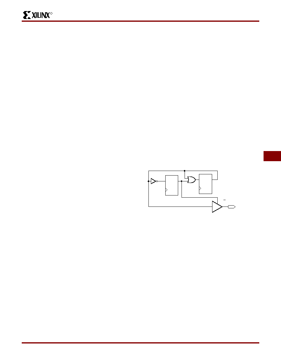
provides a solution for that case.
This solution requires one CLB, one IOB and pin, and an
internal oscillator with a frequency of up to 5 MHz as a
clock source. The XC3000 master device must be cong-
ured with late Internal Reset, which is the default option.
One CLB and one IOB in the lead XC3000-family device
are used to generate the additional CCLK pulse required by
the XC4000 Series devices. When the lead device removes
the internal RESET signal, the 2-bit shift register responds
to its clock input and generates an active Low output signal
for the duration of the subsequent clock period. An external
connection between this output and CCLK thus creates the
extra CCLK pulse.
Output
Connected
to CCLK
OE/T
0
1
0
.
0
1
.
Reset
X5223
etc
Active Low Output
Active High Output
Figure 44: CCLK Generation for XC3000 Master
Driving an XC4000 Series Slave
Product Obsolete or Under Obsolescence
相关PDF资料 |
PDF描述 |
|---|---|
| KMPC850DECVR66BU | IC MPU PWRQUICC 66MHZ 256-PBGA |
| RMC40DTEH | CONN EDGECARD 80POS .100 EYELET |
| IDT70V9389L9PRFI8 | IC SRAM 1.125MBIT 9NS 128TQFP |
| KMPC8343EZQAGD | IC MPU PWRQUICC II 620-PBGA |
| ASM28DREN | CONN EDGECARD 56POS .156 EYELET |
相关代理商/技术参数 |
参数描述 |
|---|---|
| XC4044XL-2HQ160I | 功能描述:IC FPGA I-TEMP 3.3V 2SPD 160HQFP RoHS:否 类别:集成电路 (IC) >> 嵌入式 - FPGA(现场可编程门阵列) 系列:XC4000E/X 标准包装:1 系列:Kintex-7 LAB/CLB数:25475 逻辑元件/单元数:326080 RAM 位总计:16404480 输入/输出数:350 门数:- 电源电压:0.97 V ~ 1.03 V 安装类型:表面贴装 工作温度:0°C ~ 85°C 封装/外壳:900-BBGA,FCBGA 供应商设备封装:900-FCBGA(31x31) 其它名称:122-1789 |
| XC4044XL2HQ208C | 制造商:XILINX 功能描述:* |
| XC4044XL-2HQ208C | 功能描述:IC FPGA C-TEMP 3.3V 2SPD 208HQFP RoHS:否 类别:集成电路 (IC) >> 嵌入式 - FPGA(现场可编程门阵列) 系列:XC4000E/X 标准包装:1 系列:Kintex-7 LAB/CLB数:25475 逻辑元件/单元数:326080 RAM 位总计:16404480 输入/输出数:350 门数:- 电源电压:0.97 V ~ 1.03 V 安装类型:表面贴装 工作温度:0°C ~ 85°C 封装/外壳:900-BBGA,FCBGA 供应商设备封装:900-FCBGA(31x31) 其它名称:122-1789 |
| XC4044XL-2HQ208I | 功能描述:IC FPGA I-TEMP 3.3V 2SPD 208HQFP RoHS:否 类别:集成电路 (IC) >> 嵌入式 - FPGA(现场可编程门阵列) 系列:XC4000E/X 标准包装:1 系列:Kintex-7 LAB/CLB数:25475 逻辑元件/单元数:326080 RAM 位总计:16404480 输入/输出数:350 门数:- 电源电压:0.97 V ~ 1.03 V 安装类型:表面贴装 工作温度:0°C ~ 85°C 封装/外壳:900-BBGA,FCBGA 供应商设备封装:900-FCBGA(31x31) 其它名称:122-1789 |
| XC4044XL2HQ240 | 制造商:n/a 功能描述:_ |
发布紧急采购,3分钟左右您将得到回复。