参数资料
| 型号: | XC4044XL-3HQ208C |
| 厂商: | Xilinx Inc |
| 文件页数: | 36/68页 |
| 文件大小: | 0K |
| 描述: | IC FPGA C-TEMP 3.3V 3SPD 208HQFP |
| 产品变化通告: | XC4000XL/E, XC9500XV, XC3100A Discontinuance 12/Apr/2010 |
| 标准包装: | 24 |
| 系列: | XC4000E/X |
| LAB/CLB数: | 1600 |
| 逻辑元件/单元数: | 3800 |
| RAM 位总计: | 51200 |
| 输入/输出数: | 160 |
| 门数: | 44000 |
| 电源电压: | 3 V ~ 3.6 V |
| 安装类型: | 表面贴装 |
| 工作温度: | 0°C ~ 85°C |
| 封装/外壳: | 208-BFQFP 裸露焊盘 |
| 供应商设备封装: | 208-PQFP(28x28) |
第1页第2页第3页第4页第5页第6页第7页第8页第9页第10页第11页第12页第13页第14页第15页第16页第17页第18页第19页第20页第21页第22页第23页第24页第25页第26页第27页第28页第29页第30页第31页第32页第33页第34页第35页当前第36页第37页第38页第39页第40页第41页第42页第43页第44页第45页第46页第47页第48页第49页第50页第51页第52页第53页第54页第55页第56页第57页第58页第59页第60页第61页第62页第63页第64页第65页第66页第67页第68页
R
May 14, 1999 (Version 1.6)
6-45
XC4000E and XC4000X Series Field Programmable Gate Arrays
6
Table 17: Boundary Scan Instructions
Avoiding Inadvertent Boundary Scan
If TMS or TCK is used as user I/O, care must be taken to
ensure that at least one of these pins is held constant dur-
ing conguration. In some applications, a situation may
occur where TMS or TCK is driven during conguration.
This may cause the device to go into boundary scan mode
and disrupt the conguration process.
To prevent activation of boundary scan during congura-
tion, do either of the following:
TMS: Tie High to put the Test Access Port controller
in a benign RESET state
TCK: Tie High or Low—don't toggle this clock input.
For more information regarding boundary scan, refer to the
Xilinx Application Note XAPP 017.001, “
Boundary Scan in
XC4000E Devices.“
Conguration
Conguration is the process of loading design-specic pro-
gramming data into one or more FPGAs to dene the func-
tional
operation
of
the
internal
blocks
and
their
interconnections. This is somewhat like loading the com-
mand registers of a programmable peripheral chip. XC4000
Series devices use several hundred bits of conguration
data per CLB and its associated interconnects. Each con-
guration bit denes the state of a static memory cell that
controls either a function look-up table bit, a multiplexer
input, or an interconnect pass transistor. The XACT
step
development system translates the design into a netlist le.
It automatically partitions, places and routes the logic and
generates the conguration data in PROM format.
Special Purpose Pins
Three conguration mode pins (M2, M1, M0) are sampled
prior to conguration to determine the conguration mode.
After conguration, these pins can be used as auxiliary
connections. M2 and M0 can be used as inputs, and M1
can be used as an output. The XACT
step development sys-
tem does not use these resources unless they are explicitly
specied in the design entry. This is done by placing a spe-
cial pad symbol called MD2, MD1, or MD0 instead of the
input or output pad symbol.
In XC4000 Series devices, the mode pins have weak
pull-up resistors during conguration. With all three mode
pins High, Slave Serial mode is selected, which is the most
popular conguration mode. Therefore, for the most com-
mon conguration mode, the mode pins can be left uncon-
nected. (Note, however, that the internal pull-up resistor
value can be as high as 100 k
.) After conguration, these
pins can individually have weak pull-up or pull-down resis-
tors, as specied in the design. A pull-down resistor value
of 4.7 k
is recommended.
These pins are located in the lower left chip corner and are
near the readback nets. This location allows convenient
routing if compatibility with the XC2000 and XC3000 family
conventions of M0/RT, M1/RD is desired.
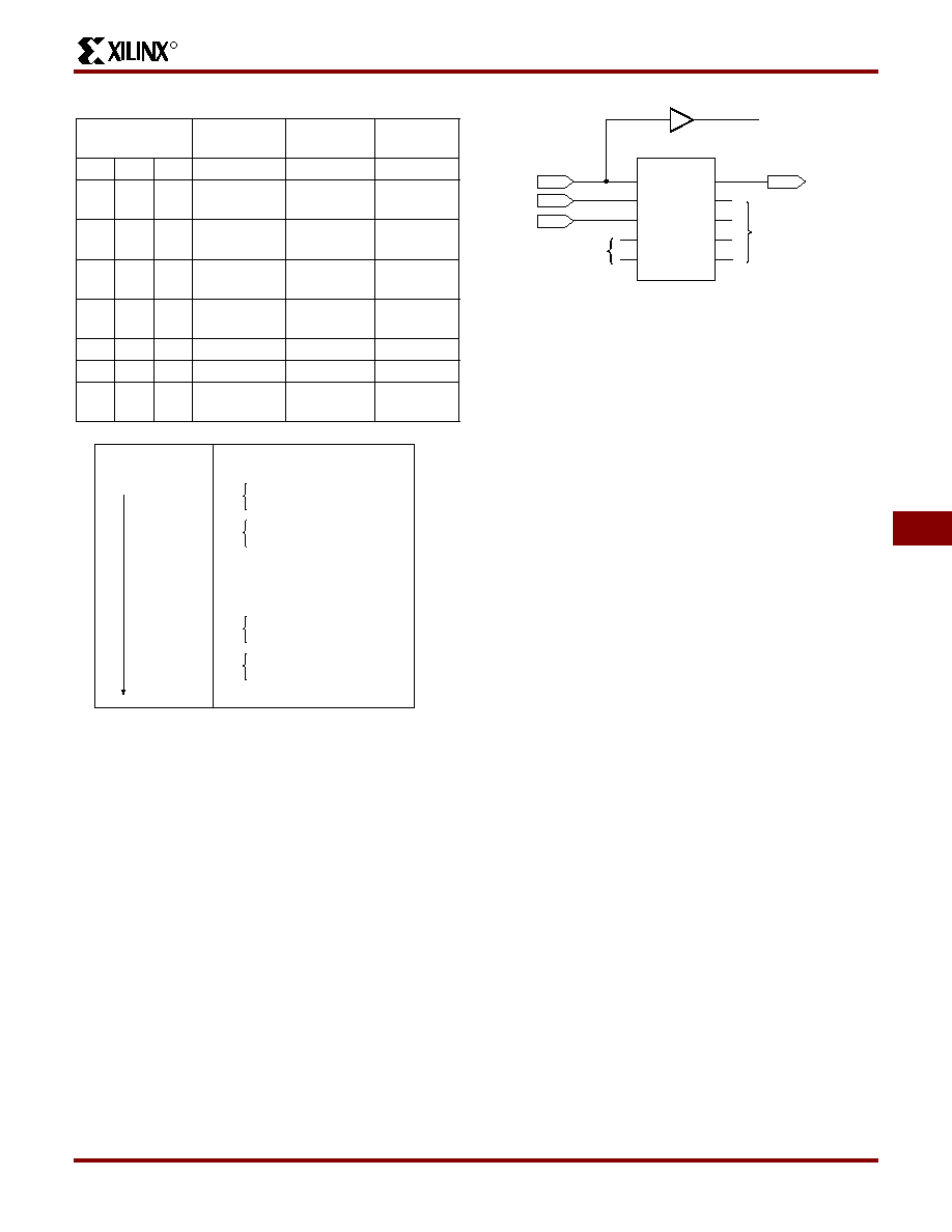
Instruction I2
I1
I0
Test
Selected
TDO Source
I/O Data
Source
0
EXTEST
DR
0
1
SAMPLE/PR
ELOAD
DR
Pin/Logic
0
1
0
USER 1
BSCAN.
TDO1
User Logic
0
1
USER 2
BSCAN.
TDO2
User Logic
1
0
READBACK
Readback
Data
Pin/Logic
1
0
1
CONFIGURE
DOUT
Disabled
1
0
Reserved
—
1
BYPASS
Bypass
Register
—
Bit 0 ( TDO end)
Bit 1
Bit 2
TDO.T
TDO.O
Top-edge IOBs (Right to Left)
Left-edge IOBs (Top to Bottom)
MD1.T
MD1.O
MD1.I
MD0.I
MD2.I
Bottom-edge IOBs (Left to Right)
Right-edge IOBs (Bottom to Top)
B SCANT.UPD
(TDI end)
X6075
Figure 42:
Boundary Scan Bit Sequence
TDI
TMS
TCK
TDO1
TDO2
TDO
DRCK
IDLE
SEL1
SEL2
TDI
TMS
TCK
TDO
BSCAN
To User
Logic
IBUF
Optional
From
User Logic
To User
Logic
X2675
Figure 43: Boundary Scan Schematic Example
Product Obsolete or Under Obsolescence
相关PDF资料 |
PDF描述 |
|---|---|
| XC4044XL-3HQ160I | IC FPGA I-TEMP 3.3V 3SPD 160HQFP |
| IDT71V30S55TF8 | IC SRAM 8KBIT 55NS 64TQFP |
| 65801-139LF | CLINCHER RECEPTACLE ASSY GOLD |
| FMC28DRYN | CONN EDGECARD 56POS DIP .100 SLD |
| 65801-113LF | CLINCHER RECEPTACLE ASSY TIN |
相关代理商/技术参数 |
参数描述 |
|---|---|
| XC4044XL-3HQ208I | 功能描述:IC FPGA I-TEMP 3.3V 3SPD 208HQFP RoHS:否 类别:集成电路 (IC) >> 嵌入式 - FPGA(现场可编程门阵列) 系列:XC4000E/X 标准包装:1 系列:Kintex-7 LAB/CLB数:25475 逻辑元件/单元数:326080 RAM 位总计:16404480 输入/输出数:350 门数:- 电源电压:0.97 V ~ 1.03 V 安装类型:表面贴装 工作温度:0°C ~ 85°C 封装/外壳:900-BBGA,FCBGA 供应商设备封装:900-FCBGA(31x31) 其它名称:122-1789 |
| XC4044XL-3HQ240C | 功能描述:IC FPGA C-TEMP 3.3V 3SPD 240HQFP RoHS:否 类别:集成电路 (IC) >> 嵌入式 - FPGA(现场可编程门阵列) 系列:XC4000E/X 标准包装:1 系列:Kintex-7 LAB/CLB数:25475 逻辑元件/单元数:326080 RAM 位总计:16404480 输入/输出数:350 门数:- 电源电压:0.97 V ~ 1.03 V 安装类型:表面贴装 工作温度:0°C ~ 85°C 封装/外壳:900-BBGA,FCBGA 供应商设备封装:900-FCBGA(31x31) 其它名称:122-1789 |
| XC4044XL-3HQ240I | 功能描述:IC FPGA I-TEMP 3.3V 3SPD 240HQFP RoHS:否 类别:集成电路 (IC) >> 嵌入式 - FPGA(现场可编程门阵列) 系列:XC4000E/X 标准包装:1 系列:Kintex-7 LAB/CLB数:25475 逻辑元件/单元数:326080 RAM 位总计:16404480 输入/输出数:350 门数:- 电源电压:0.97 V ~ 1.03 V 安装类型:表面贴装 工作温度:0°C ~ 85°C 封装/外壳:900-BBGA,FCBGA 供应商设备封装:900-FCBGA(31x31) 其它名称:122-1789 |
| XC4044XL-3HQ304C | 功能描述:IC FPGA C-TEMP 3.3V 3SPD 304HQFP RoHS:否 类别:集成电路 (IC) >> 嵌入式 - FPGA(现场可编程门阵列) 系列:XC4000E/X 标准包装:1 系列:Kintex-7 LAB/CLB数:25475 逻辑元件/单元数:326080 RAM 位总计:16404480 输入/输出数:350 门数:- 电源电压:0.97 V ~ 1.03 V 安装类型:表面贴装 工作温度:0°C ~ 85°C 封装/外壳:900-BBGA,FCBGA 供应商设备封装:900-FCBGA(31x31) 其它名称:122-1789 |
| XC4044XL-3HQ304I | 功能描述:IC FPGA I-TEMP 3.3V 3SPD 304HQFP RoHS:否 类别:集成电路 (IC) >> 嵌入式 - FPGA(现场可编程门阵列) 系列:XC4000E/X 标准包装:1 系列:Kintex-7 LAB/CLB数:25475 逻辑元件/单元数:326080 RAM 位总计:16404480 输入/输出数:350 门数:- 电源电压:0.97 V ~ 1.03 V 安装类型:表面贴装 工作温度:0°C ~ 85°C 封装/外壳:900-BBGA,FCBGA 供应商设备封装:900-FCBGA(31x31) 其它名称:122-1789 |
发布紧急采购,3分钟左右您将得到回复。