- 您现在的位置:买卖IC网 > PDF目录225572 > XC4VFX100-10FF1517I (XILINX INC) FPGA, 10544 CLBS, 1028 MHz, PBGA1517 PDF资料下载
参数资料
| 型号: | XC4VFX100-10FF1517I |
| 厂商: | XILINX INC |
| 元件分类: | FPGA |
| 英文描述: | FPGA, 10544 CLBS, 1028 MHz, PBGA1517 |
| 封装: | FBGA-1517 |
| 文件页数: | 25/58页 |
| 文件大小: | 1863K |
| 代理商: | XC4VFX100-10FF1517I |
第1页第2页第3页第4页第5页第6页第7页第8页第9页第10页第11页第12页第13页第14页第15页第16页第17页第18页第19页第20页第21页第22页第23页第24页当前第25页第26页第27页第28页第29页第30页第31页第32页第33页第34页第35页第36页第37页第38页第39页第40页第41页第42页第43页第44页第45页第46页第47页第48页第49页第50页第51页第52页第53页第54页第55页第56页第57页第58页
Virtex-4 FPGA Data Sheet: DC and Switching Characteristics
DS302 (v3.7) September 9, 2009
Product Specification
31
CLB Switching Characteristics
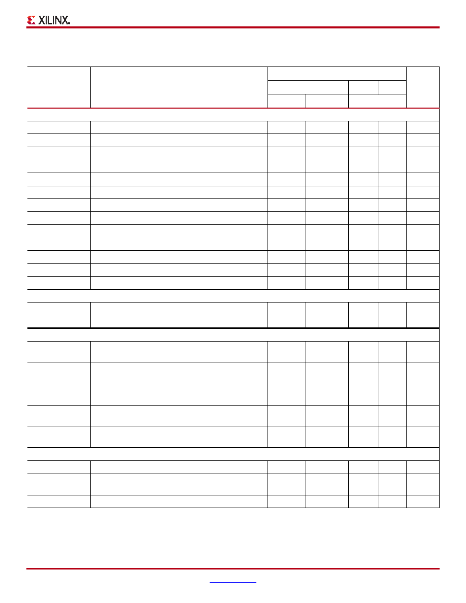
Table 37: CLB Switching Characteristics
Symbol
Description
Speed Grade
Units
-12
-11
-10
XC4VFX(2)
XC4VLX/SX
ALL DEVICES
Combinatorial Delays
TILO
4-input function: F/G inputs to X/Y outputs
0.15
0.17
0.20
ns, Max
TIF5
5-input function: F/G inputs to F5 output
0.36
0.35
0.40
0.46
ns, Max
TIF5X
5-input function: F/G inputs to X output
0.44
0.43
0.49
0.57
ns, Max
TIF6Y
FXINA or FXINB inputs to YMUX output
0.30
0.34
0.39
ns, Max
TINAFX
FXINA input to FX output via MUXFX
0.21
0.23
0.27
ns, Max
TINBFX
FXINB input to FX output via MUXFX
0.21
0.20
0.23
0.26
ns, Max
TBXX
BX input to XMUX output
0.59
0.58
0.65
0.76
ns, Max
TBYY
BY input to YMUX output
0.43
0.48
0.56
ns, Max
TBXCY
BX input to COUT output – Getting into carry chain(3)
0.60
0.59
0.66
0.78
ns, Max
TBYCY
BY input to COUT output – Getting into carry chain(3)
0.49
0.48
0.54
0.63
ns, Max
TBYP
CIN input to COUT output – Carry chain delay(3)
0.07
0.08
0.09
ns, Max
TOPCYF
F input to COUT output – Getting out from carry chain(3)
0.45
0.44
0.50
0.58
ns, Max
TOPCYG
G input to COUT output – Getting out from carry chain(3)
0.44
0.43
0.48
0.57
ns, Max
Sequential Delays
TCKO
FF Clock CLK to XQ/YQ outputs
0.28
0.31
0.36
ns, Max
TCKLO
Latch Clock CLK to XQ/YQ outputs
0.37
0.36
0.41
0.48
ns, Max
Setup and Hold Times of CLB Flip-Flops Before/After Clock CLK
TDICK / TCKDI
BX/BY inputs
0.36
–0.09
0.36
–0.09
0.40
–0.09
0.47
–0.09
ns, Min
TCECK / TCKCE
CE input
0.58
–0.16
0.57
–0.16
0.64
–0.16
0.75
–0.16
ns, Min
TFXCK / TCKFX
FXINA/FXINB inputs
0.42
–0.14
0.41
–0.14
0.46
–0.14
0.54
–0.14
ns, Min
TSRCK / TCKSR
SR/BY inputs (synchronous)
1.04
–0.74
1.02
–0.73
1.15
–0.73
1.35
–0.73
ns, Min
TCINCK / TCKCIN
CIN Data Inputs (DI) – Getting out from carry chain(3)
0.52
–0.23
0.51
–0.23
0.57
–0.23
0.67
–0.23
ns, Min
Set/Reset
TRPW
Minimum Pulse Width, SR/BY inputs
0.54
0.53
0.59
0.70
ns, Min
TRQ
Delay from SR/BY inputs to XQ/YQ outputs
(asynchronous)
1.05
1.03
1.15
1.35
ns, Max
FTOG
Toggle Frequency (MHz) (for export control)
1181
1205
1205(4)
1028
MHz
Notes:
1.
A Zero “0” Hold Time listing indicates no hold time or a negative hold time. Negative values cannot be guaranteed “best-case,” but if a “0” is listed,
there is no positive hold time.
2.
The values in this column apply to all XC4VFX -12 parts except XC4VFX12 -12. For XC4VFX12 -12 values, use the values in the adjacent 4VLX/SX
-12 column.
3.
These items are of interest for Carry Chain applications.
4.
XC4VFX -11 devices are 1181 MHz.
相关PDF资料 |
PDF描述 |
|---|---|
| XC4VFX100-11FF1152I | FPGA, 10544 CLBS, 1181 MHz, PBGA1152 |
| XC4VFX100-11FF1517I | FPGA, 10544 CLBS, 1181 MHz, PBGA1517 |
| XC4VFX100-10FFG1152I | FPGA, 10544 CLBS, 1028 MHz, PBGA1152 |
| XC4VFX100-10FFG1517I | FPGA, 10544 CLBS, 1028 MHz, PBGA1517 |
| XC4VFX100-11FFG1152I | FPGA, 10544 CLBS, 1181 MHz, PBGA1152 |
相关代理商/技术参数 |
参数描述 |
|---|---|
| XC4VFX100-10FF1517I4020 | 制造商:Xilinx 功能描述: |
| XC4VFX100-10FF1517IES1 | 制造商:Xilinx 功能描述: |
| XC4VFX100-10FFG1152C | 功能描述:IC FPGA VIRTEX-4FX 100K 1152FBGA RoHS:是 类别:集成电路 (IC) >> 嵌入式 - FPGA(现场可编程门阵列) 系列:Virtex®-4 FX 产品变化通告:XC4000(E,L) Discontinuation 01/April/2002 标准包装:24 系列:XC4000E/X LAB/CLB数:100 逻辑元件/单元数:238 RAM 位总计:3200 输入/输出数:80 门数:3000 电源电压:4.5 V ~ 5.5 V 安装类型:表面贴装 工作温度:-40°C ~ 100°C 封装/外壳:120-BCBGA 供应商设备封装:120-CPGA(34.55x34.55) |
| XC4VFX100-10FFG1152I | 功能描述:IC FPGA VIRTEX-4FX 100K 1152FBGA RoHS:是 类别:集成电路 (IC) >> 嵌入式 - FPGA(现场可编程门阵列) 系列:Virtex®-4 FX 产品变化通告:XC4000(E,L) Discontinuation 01/April/2002 标准包装:24 系列:XC4000E/X LAB/CLB数:100 逻辑元件/单元数:238 RAM 位总计:3200 输入/输出数:80 门数:3000 电源电压:4.5 V ~ 5.5 V 安装类型:表面贴装 工作温度:-40°C ~ 100°C 封装/外壳:120-BCBGA 供应商设备封装:120-CPGA(34.55x34.55) |
| XC4VFX100-10FFG1517C | 功能描述:IC FPGA VIRTEX-4FX 100K 1517FBGA RoHS:是 类别:集成电路 (IC) >> 嵌入式 - FPGA(现场可编程门阵列) 系列:Virtex®-4 FX 产品变化通告:XC4000(E,L) Discontinuation 01/April/2002 标准包装:24 系列:XC4000E/X LAB/CLB数:100 逻辑元件/单元数:238 RAM 位总计:3200 输入/输出数:80 门数:3000 电源电压:4.5 V ~ 5.5 V 安装类型:表面贴装 工作温度:-40°C ~ 100°C 封装/外壳:120-BCBGA 供应商设备封装:120-CPGA(34.55x34.55) |
发布紧急采购,3分钟左右您将得到回复。