- 您现在的位置:买卖IC网 > PDF目录225572 > XC4VFX100-10FF1517I (XILINX INC) FPGA, 10544 CLBS, 1028 MHz, PBGA1517 PDF资料下载
参数资料
| 型号: | XC4VFX100-10FF1517I |
| 厂商: | XILINX INC |
| 元件分类: | FPGA |
| 英文描述: | FPGA, 10544 CLBS, 1028 MHz, PBGA1517 |
| 封装: | FBGA-1517 |
| 文件页数: | 27/58页 |
| 文件大小: | 1863K |
| 代理商: | XC4VFX100-10FF1517I |
第1页第2页第3页第4页第5页第6页第7页第8页第9页第10页第11页第12页第13页第14页第15页第16页第17页第18页第19页第20页第21页第22页第23页第24页第25页第26页当前第27页第28页第29页第30页第31页第32页第33页第34页第35页第36页第37页第38页第39页第40页第41页第42页第43页第44页第45页第46页第47页第48页第49页第50页第51页第52页第53页第54页第55页第56页第57页第58页
Virtex-4 FPGA Data Sheet: DC and Switching Characteristics
DS302 (v3.7) September 9, 2009
Product Specification
33
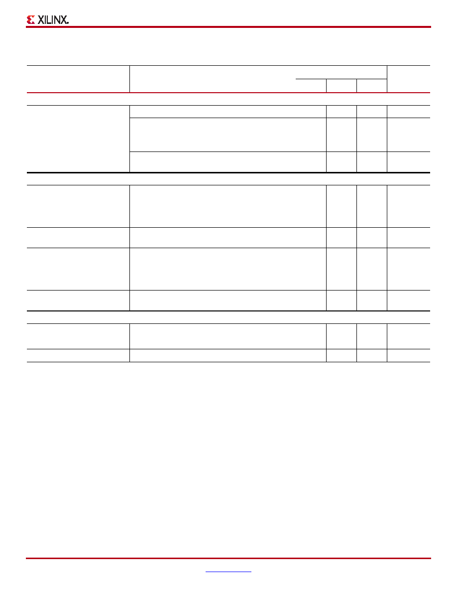
Block RAM and FIFO Switching Characteristics
Table 40: Block RAM Switching Characteristics
Symbol
Description
Speed Grade
Units
-12
-11
-10
Sequential Delays
TRCKO_DORA
Clock CLK to DOUT output (without output register)(2)
1.65
1.83
2.10
ns, Max
Clock CLK to DOUT output with ECC
(without output register)
3.00
3.33
3.83
ns, Max
TRCKO_DOA
Clock CLK to DOUT output (with output register)(3)
0.72
0.80
0.92
ns, Max
Clock CLK to DOUT output with ECC (with output
register)
2.00
2.20
2.50
ns, Max
Setup and Hold Times Before Clock CLK
TRCCK_ADDR / TRCKC_ADDR
ADDR inputs
0.34
0.26
0.37
0.28
0.43
0.33
ns, Min
TRDCK_DI / TRCKD_DI
DIN inputs(4)
0.18
0.26
0.20
0.28
0.23
0.33
ns, Min
TRCCK_EN / TRCKC_EN
EN input(5)
0.41
0.26
0.45
0.28
0.52
0.33
ns, Min
TRCCK_REGCE /TRCKC_REGCE
CE input of output register
0.25
0.26
0.27
0.28
0.32
0.33
ns, Min
TRCCK_SSR / TRCKC_SSR
RST input
0.25
0.26
0.27
0.28
0.32
0.33
ns, Min
TRCCK_WE / TRCKC_WE
WEN input
0.59
0.26
0.65
0.28
0.75
0.33
ns, Min
Maximum Frequency
FMAX
Write first and no change mode
500.00
450.45
400.00
MHz
FMAX
Read first mode
500.00
450.45
400.00
MHz
CLK-to-CLK
Read first mode
500.00
450.45
400.00
MHz
Notes:
1.
A Zero “0” Hold Time listing indicates no hold time or a negative hold time. Negative values cannot be guaranteed “best-case,” but if a “0” is listed,
there is no positive hold time.
2.
TRCKO_DORA includes TRCKO_DOWA, TRCKO_DOPAR, and TRCKO_DOPAW as well as the B port equivalent timing parameters.
3.
TRCKO_DOA includes TRCKO_DOPA as well as the B port equivalent timing parameters.
4.
TRCKO_DI includes both A and B inputs as well as the parity inputs of A and B.
5.
Xilinx block RAMs do not have asynchronous inputs on an enabled port address. During the time that a port is enabled, its addresses must be stable
during the specified set-up time. Do not create an asynchronous input on an enabled port address.
相关PDF资料 |
PDF描述 |
|---|---|
| XC4VFX100-11FF1152I | FPGA, 10544 CLBS, 1181 MHz, PBGA1152 |
| XC4VFX100-11FF1517I | FPGA, 10544 CLBS, 1181 MHz, PBGA1517 |
| XC4VFX100-10FFG1152I | FPGA, 10544 CLBS, 1028 MHz, PBGA1152 |
| XC4VFX100-10FFG1517I | FPGA, 10544 CLBS, 1028 MHz, PBGA1517 |
| XC4VFX100-11FFG1152I | FPGA, 10544 CLBS, 1181 MHz, PBGA1152 |
相关代理商/技术参数 |
参数描述 |
|---|---|
| XC4VFX100-10FF1517I4020 | 制造商:Xilinx 功能描述: |
| XC4VFX100-10FF1517IES1 | 制造商:Xilinx 功能描述: |
| XC4VFX100-10FFG1152C | 功能描述:IC FPGA VIRTEX-4FX 100K 1152FBGA RoHS:是 类别:集成电路 (IC) >> 嵌入式 - FPGA(现场可编程门阵列) 系列:Virtex®-4 FX 产品变化通告:XC4000(E,L) Discontinuation 01/April/2002 标准包装:24 系列:XC4000E/X LAB/CLB数:100 逻辑元件/单元数:238 RAM 位总计:3200 输入/输出数:80 门数:3000 电源电压:4.5 V ~ 5.5 V 安装类型:表面贴装 工作温度:-40°C ~ 100°C 封装/外壳:120-BCBGA 供应商设备封装:120-CPGA(34.55x34.55) |
| XC4VFX100-10FFG1152I | 功能描述:IC FPGA VIRTEX-4FX 100K 1152FBGA RoHS:是 类别:集成电路 (IC) >> 嵌入式 - FPGA(现场可编程门阵列) 系列:Virtex®-4 FX 产品变化通告:XC4000(E,L) Discontinuation 01/April/2002 标准包装:24 系列:XC4000E/X LAB/CLB数:100 逻辑元件/单元数:238 RAM 位总计:3200 输入/输出数:80 门数:3000 电源电压:4.5 V ~ 5.5 V 安装类型:表面贴装 工作温度:-40°C ~ 100°C 封装/外壳:120-BCBGA 供应商设备封装:120-CPGA(34.55x34.55) |
| XC4VFX100-10FFG1517C | 功能描述:IC FPGA VIRTEX-4FX 100K 1517FBGA RoHS:是 类别:集成电路 (IC) >> 嵌入式 - FPGA(现场可编程门阵列) 系列:Virtex®-4 FX 产品变化通告:XC4000(E,L) Discontinuation 01/April/2002 标准包装:24 系列:XC4000E/X LAB/CLB数:100 逻辑元件/单元数:238 RAM 位总计:3200 输入/输出数:80 门数:3000 电源电压:4.5 V ~ 5.5 V 安装类型:表面贴装 工作温度:-40°C ~ 100°C 封装/外壳:120-BCBGA 供应商设备封装:120-CPGA(34.55x34.55) |
发布紧急采购,3分钟左右您将得到回复。