- 您现在的位置:买卖IC网 > PDF目录205968 > XC6405B (TOREX SEMICONDUCTOR LTD.) High Current, High Speed LDO Regulators, Voltage Detector Function PDF资料下载
参数资料
| 型号: | XC6405B |
| 厂商: | TOREX SEMICONDUCTOR LTD. |
| 元件分类: | 线性稳压 |
| 英文描述: | High Current, High Speed LDO Regulators, Voltage Detector Function |
| 中文描述: | 高电流,高速LDO稳压器,电压检测功能 |
| 文件页数: | 18/54页 |
| 文件大小: | 558K |
| 代理商: | XC6405B |
第1页第2页第3页第4页第5页第6页第7页第8页第9页第10页第11页第12页第13页第14页第15页第16页第17页当前第18页第19页第20页第21页第22页第23页第24页第25页第26页第27页第28页第29页第30页第31页第32页第33页第34页第35页第36页第37页第38页第39页第40页第41页第42页第43页第44页第45页第46页第47页第48页第49页第50页第51页第52页第53页第54页
XC6405 Series
High Current, High Speed LDO Regulators, Voltage Detector Function
! OPERATIONAL EXPLANATION (Continued)
<EN / CE Pin>
( * A ~ D Series)
<Toggle Operation>
XC6405 * E ~ K
Active HIGH with no pull down
XC6405 * L ~ P
Input Current = VIN voltage / Pull Up Resistance
In stand-by mode, the above input current can be reduced by connecting a pull-up resistor between VROUT and VDOUT.
Note that as the XC6405*E to K types of the XC6405A to D series are 'Active HIGH / No Pull Down' and XC6405*R to U types of the XC6405A to D
series are 'Active LOW / No Pull Up', operations will become unstable with the CE pin open (See the chart below).
SERIES
EN/CE INPUT LOGIC
EN Logic Active "HIGH"
The IC's internal regulator circuitry can be shut down via the signal from the EN pin with the XC6405A, B, C series. In shutdown mode, output at the
VROUT pin will be pulled down to the VSS level via R1 & R2. The whole IC's circuitry can be shut down via CE pin with the XC6405D series and power
consumption can be reduced to around 0
A. While the voltage detector is in shutdown mode, the voltage detector output is in a post-detection state.
When choosing Detect L, input current can be set by using the following formula.
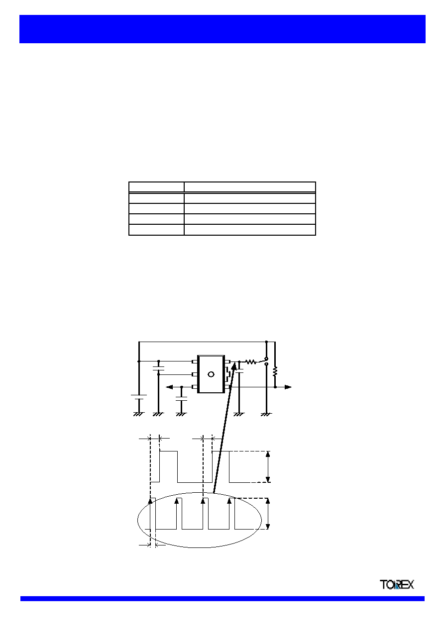
The XC6405 A and B series have a built-in toggle ON/OFF switch which repeats an on/off operation via the EN pin's leading edge signal when the EN
logic is Active HIGH, and via the EN pin's falling edge signal when the EN logic is Active LOW (Please also refer the figure below). The EN input signal
duration should be over 500nsec. If the EN input signal is less than 500nsec, it is possible that the circuit fails to respond and the toggle function does
not operate. To operate the toggle function properly when the EN pin voltage noise is large, a RC filter should be used to reduce the noise in the signal
to the EN pin. In the case where input delay time is required, it is possible to set the time constant by connecting an RC network to the EN pin.
We suggest that you use this IC with either a VIN voltage or a VSS voltage input at the EN or CE pin. If this IC is used with the correct specifications for
the EN or CE pin, the IC will operate normally. However, supply current may increase as a result of through current in the IC's internal circuitry if a
voltage other than VIN or VSS is applied.
Active LOW with pull up
XC6405 * R ~ U
Active LOW with no pull up
XC6405 * A ~ D
Active HIGH with pull down
Semiconductor Ltd.
Rpull
220k
CIN
1uF
1.5k
0.1uF
VIN
VIN Voltage
GND
EN pin signal
VROUT Voltage
GND
More than
500nsec
Internal Circuit - Response time
apporx. 10usec.
VIN
VSS
EN
VROUT
VDOUT
1uF
CL
Data Sheet
25
相关PDF资料 |
PDF描述 |
|---|---|
| XC6405C | High Current, High Speed LDO Regulators, Voltage Detector Function |
| XC74WL04AASR | CMOS Logic Triple Inverter |
| XC95108-7PC84I | XC95108 In-System Programmable CPLD |
| XC95108-7PQ100C | XC95108 In-System Programmable CPLD |
| XC95108-7PQ100I | XC95108 In-System Programmable CPLD |
相关代理商/技术参数 |
参数描述 |
|---|---|
| XC6405C | 制造商:TOREX 制造商全称:Torex Semiconductor 功能描述:High Current, High Speed LDO Regulators, Voltage Detector Function |
| XC6405CE81MR | 制造商:TOREX 制造商全称:Torex Semiconductor 功能描述:High Current, High Speed LDO Regulators, Voltage Detector Function |
| XC6405CH80MR | 制造商:TOREX 制造商全称:Torex Semiconductor 功能描述:High Current, High Speed LDO Regulators, Voltage Detector Function |
| XC6405D | 制造商:TOREX 制造商全称:Torex Semiconductor 功能描述:High Current, High Speed LDO Regulators, Voltage Detector Function |
| XC6405DE82MR | 制造商:TOREX 制造商全称:Torex Semiconductor 功能描述:High Current, High Speed LDO Regulators, Voltage Detector Function |
发布紧急采购,3分钟左右您将得到回复。