- 您现在的位置:买卖IC网 > PDF目录1883 > XC9235A33DER-G (Torex Semiconductor Ltd)IC REG BUCK SYNC 3.3V 0.6A USP-6 PDF资料下载
参数资料
| 型号: | XC9235A33DER-G |
| 厂商: | Torex Semiconductor Ltd |
| 文件页数: | 8/34页 |
| 文件大小: | 0K |
| 描述: | IC REG BUCK SYNC 3.3V 0.6A USP-6 |
| 标准包装: | 3,000 |
| 类型: | 降压(降压) |
| 输出类型: | 固定 |
| 输出数: | 1 |
| 输出电压: | 3.3V |
| 输入电压: | 2 V ~ 6 V |
| 频率 - 开关: | 3MHz |
| 电流 - 输出: | 600mA |
| 同步整流器: | 是 |
| 工作温度: | -40°C ~ 85°C |
| 安装类型: | 表面贴装 |
| 封装/外壳: | 6-UFDFN 裸露焊盘 |
| 包装: | 带卷 (TR) |
| 供应商设备封装: | USP-6C |
第1页第2页第3页第4页第5页第6页第7页当前第8页第9页第10页第11页第12页第13页第14页第15页第16页第17页第18页第19页第20页第21页第22页第23页第24页第25页第26页第27页第28页第29页第30页第31页第32页第33页第34页
�� �
�
�XC9235/XC9236/XC9237� Series�
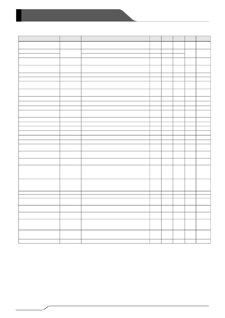
�■� ELECTRICAL� CHARACTERISTICS� (Continued)�
�XC9235B(C)(E)(G)18Dxx/XC9236B(C)(E)(G)18Dxx/XC9237B(C)(E)(G)18Dxx,� V� OUT� =1.8V,� f� OSC� =3.0MHz,� Ta=25� ℃�
�PARAMETER�
�Output� Voltage�
�Operating Voltage Range (B/C series)�
�Operating Voltage Range (E/G series)�
�SYMBOL�
�V� OUT�
�V� IN�
�CONDITIONS�
�When� connected� to� external� components,�
�V� IN� =V� CE� =5.0V,� I� OUT� =30mA�
�MIN.�
�1.764�
�2.0�
�1.8�
�TYP.�
�1.800�
�-�
�-�
�MAX.�
�1.836�
�6.0�
�6.0�
�UNIT�
�V�
�V�
�CIRCUIT�
�①�
�①�
�Maximum� Output� Current�
�I� OUTMAX�
�V� IN� =V� OUT(E)� +2.0V,� V� CE� =1.0V,�
�When� connected� to� external� components�
�(*9)�
�600�
�-�
�-�
�mA�
�①�
�V� CE� =V� IN� ,� V� OUT� =V� OUT(E)� � 0.5V�
�,�
�UVLO� Voltage�
�V� UVLO�
�(*14)�
�Voltage� which� Lx� pin� holding� “L”� level�
�(*1,*11)�
�1.00�
�1.40�
�1.78�
�V�
�③�
�V� IN� =V� OUT(E)� +2.0V,� V� CE� =V� IN� ,� I� OUT� =1mA�
�Supply� Current�
�Stand-by� Current�
�Oscillation� Frequency�
�PFM� Switching� Current�
�I� DD�
�I� STB�
�f� OSC�
�I� PFM�
�V� IN� =V� CE� =5.0V,� V� OUT� =V� OUT(E)� � 1.1V�
�V� IN� =5.0V,� V� CE� =0V,� V� OUT� =V� OUT(E)� � 1.1V�
�When� connected� to� external� components,�
�V� IN� =V� OUT(E)� +2.0V,� V� CE� =1.0V,� I� OUT� =100mA�
�When� connected� to� external� components,�
�(*12)�
�-�
�-�
�2550�
�170�
�21�
�0�
�3000�
�220�
�35�
�1.0�
�3450�
�270�
�μ� A�
�μ� A�
�kHz�
�mA�
�②�
�②�
�①�
�①�
�PFM� Duty� Limit�
�DTY� LIMIT_PFM�
�V� CE� =V� IN� =(C-1),� I� OUT� =1mA�
�(*12)�
�-�
�200�
�300�
�%�
�①�
�Efficiency�
�Maximum� Duty� Cycle�
�Minimum� Duty� Cycle�
�(*2)�
�DTY� MAX�
�DTY� MIN�
�EFFI�
�V� IN� =V� CE� =5.0V,� V� OUT� =V� OUT(E)� � 0.9V�
�V� IN� =V� CE� =5.0V,� V� OUT� =V� OUT(E)� � 0.1V�
�When� connected� to� external� components,�
�V� CE� =V� IN� =� V� OUT(E)� +1.2V,� I� OUT� =100mA�
�100�
�-�
�-�
�-�
�-�
�86�
�-�
�0�
�-�
�%�
�%�
�%�
�③�
�③�
�①�
�Lx� SW� "H"� ON� Resistance� 1�
�Lx� SW� "H"� ON� Resistance� 2�
�R� LxH�
�R� LxH�
�V� IN� =V� CE� =5.0V,� V� OUT� =V� OUT(E)� ×0.9V,� I� Lx� =100mA�
�V� IN� =V� CE� =3.6V,� V� OUT� =V� OUT(E)� ×0.9V,� I� Lx� =100mA�
�(*3)�
�(*3)�
�-�
�-�
�0.35�
�0.42�
�0.55�
�0.67�
�Ω�
�Ω�
�④�
�④�
�Lx� SW� "L"� ON� Resistance� 1�
�Lx� SW� "L"� ON� Resistance� 2�
�R� LxL�
�R� LxL�
�V� IN� =V� CE� =5.0V�
�V� IN� =V� CE� =3.6V�
�(*4)�
�(*4)�
�-�
�-�
�0.45�
�0.52�
�0.65�
�0.77�
�Ω�
�Ω�
�-�
�-�
�Lx� SW� "H"� Leak� Current�
�(*5)�
�I� LEAKH�
�V� IN� =V� OUT� =5.0V,� V� CE� =0V,� Lx=0V�
�-�
�0.01�
�1.0�
�μ� A�
�⑤�
�Current� Limit�
�(*10)�
�I� LIM�
�V� IN� =V� CE� =5.0V,� V� OUT� =V� OUT(E)� � 0.9V�
�(*8)�
�900�
�1050�
�1350�
�mA�
�⑥�
�Voltage� changes� Lx� to� “H”� level�
�Voltage� changes� Lx� to� “L”� level�
�I� OUT� =1mA�
�,� Voltage� which� oscillation� frequency�
�becomes� 2550kHz� ≦� f� OSC� ≦� 3450kHz�
�I� OUT� =1mA�
�,� Voltage� which� oscillation� frequency�
�becomes� f� OSC� <� 2550kHz�
�Short� Lx� at� 1� Ω� resistance�
�Output� Voltage�
�Temperature� Characteristics�
�CE� "H"� Voltage�
�CE� "L"� Voltage�
�PWM� "H"� Level� Voltage�
�PWM� "L"� Level� Voltage�
�CE� "H"� Current�
�CE� "L"� Current�
�Soft� Start� Time� (B/G� Series)�
�Soft� Start� Time� (C/E� Series)�
�Latch� Time�
�Short� Protection� Threshold�
�Voltage� (B/C� Series)�
�△� V� OUT� /�
�(V� OUT� ?△� Topr)�
�V� CEH�
�V� CEL�
�V� PWMH�
�V� PWML�
�I� CEH�
�I� CEL�
�t� SS�
�t� SS�
�t� LAT�
�V� SHORT�
�I� OUT� =30mA,� -40� ℃≦� Topr� ≦� 85� ℃�
�V� OUT� =V� OUT(E)� ×0.9V,� Applied� voltage� to� V� CE� ,�
�(*11)�
�V� OUT� =V� OUT(E)� ×0.9V,� Applied� voltage� to� V� CE� ,�
�(*11)�
�When� connected� to� external� components,�
�(*6)�
�(*13)�
�When� connected� to� external� components,�
�(*6)�
�(*13)�
�V� IN� =V� CE� =5.0V,� V� OUT� =V� OUT(E)� ×0.9V�
�V� IN� =5.0V,� V� CE� =0V,� V� OUT� =V� OUT(E)� ×0.9V�
�When� connected� to� external� components,�
�V� CE� =0V� →� V� IN� ,� I� OUT� =1mA�
�When� connected� to� external� components,�
�V� CE� =0V� →� V� IN� ,� I� OUT� =1mA�
�V� IN� =V� CE� =5.0V,� V� OUT� =0.8� � V� OUT(E)� ,�
�(*7)�
�Sweeping� V� OUT� ,� V� IN� =V� CE� =5.0V,� Short� Lx� at�
�1� Ω� resistance,� V� OUT� voltage� which� Lx� becomes�
�“L”� level� within� 1ms�
�-�
�0.65�
�V� SS�
�-�
�V� IN� –�
�0.25�
�-� 0.1�
�-� 0.1�
�-�
�0.5�
�1.0�
�0.675�
�±� 100�
�-�
�-�
�-�
�-�
�-�
�-�
�0.32�
�0.9�
�-�
�0.900�
�-�
�6.0�
�0.25�
�V� IN� -� 1.0�
�-�
�0.1�
�0.1�
�0.50�
�2.5�
�20�
�1.150�
�ppm/� ℃�
�V�
�V�
�V�
�V�
�μ� A�
�μ� A�
�ms�
�ms�
�ms�
�V�
�①�
�③�
�③�
�①�
�①�
�⑤�
�⑤�
�①�
�①�
�⑦�
�⑦�
�V� IN� =V� CE� =5.0V,� The� V� OUT� at� Lx=”Low"�
�Short� Protection� Threshold�
�Voltage� (E/G� Series)�
�C� L� Discharge�
�V� SHORT�
�R� DCHG�
�(*11)�
�decreasing� V� OUT� from� V� OUT� (E)� ×0.4V�
�V� IN� =5.0V,� L� X� =5.0V,� V� CE� =0V,� V� OUT� =open�
�while�
�0.338�
�200�
�0.450�
�300�
�0.563�
�450�
�V�
�Ω�
�⑦�
�⑧�
�Test� conditions:� Unless� otherwise� stated,� V� IN� =5.0V,� V� OUT(E)� =Nominal� Voltage,� applied� voltage� sequence� is� V� OUT� →� V� IN� →� V� CE�
�NOTE:�
�*1:� Including� hysteresis� operating� voltage� range.�
�*2:� EFFI� =� {� (� output� voltage� � output� current� )� /� (� input� voltage� � input� current)� }� � 100�
�*3:� ON� resistance� (� Ω� )=� (V� IN� -� Lx� pin� measurement� voltage)� /� 100mA�
�*4:� R&D� value�
�*5:� When� temperature� is� high,� a� current� of� approximately� 10� μ� A� (maximum)� may� leak.�
�*6:� The� CE/MODE� pin� of� the� XC9237A� series� works� also� as� an� external� switching� pin� of� PWM� control� and� PWM/PFM� control.� When� the� IC� is� in� the� operation,�
�control� is� switched� to� the� automatic� PWM/PFM� switching� mode� when� the� CE/MODE� pin� voltage� is� equal� to� or� greater� than� V� IN� minus� 0.3V,� and� to� the� PWM�
�mode� when� the� CE/MODE� pin� voltage� is� equal� to� or� lower� than� V� IN� minus� 1.0V� and� equal� to� or� greater� than� V� CEH� .�
�*7:� Time� until� it� short-circuits� V� OUT� with� GND� via� 1� Ω� of� resistor� from� an� operational� state� and� is� set� to� Lx=0V� from� current� limit� pulse� generating.�
�*8:� When� V� IN� is� less� than� 2.4V,� limit� current� may� not� be� reached� because� voltage� falls� caused� by� ON� resistance.�
�*9:� When� the� difference� between� the� input� and� the� output� is� small,� some� cycles� may� be� skipped� completely� before� current� maximizes.�
�If� current� is� further� pulled� from� this� state,� output� voltage� will� decrease� because� of� P-ch� driver� ON� resistance.�
�*10:� Current� limit� denotes� the� level� of� detection� at� peak� of� coil� current.�
�*11:� “H”=V� IN� ~V� IN� -1.2V,� “L”=+0.1V~-0.1V�
�*12:� XC9235� series� exclude� I� PFM� and� DTY� LIMIT_PFM� because� those� are� only� for� the� PFM� control’s� functions.�
�*13:� XC9235/XC9236� series� exclude� V� PWMH� and� V� PWML� because� those� are� only� for� the� XC9237� series’� functions.�
�*14:� V� IN� is� applied� when� V� OUT� (E)� x� 0.5V� becomes� more� than� V� IN� .�
�8/34�
�相关PDF资料 |
PDF描述 |
|---|---|
| XC9243B08DDR-G | IC REG BUCK SYNC ADJ 2A USP-10B |
| XC9303B093KR-G | IC REG CTRLR BST PWM 8-MSOP |
| XC9503B093AR-G | IC REG BUCK ADJ 1A DL 10MSOP |
| XC9519A12AZR-G | IC REG BOOST INV ADJ 2A DL 24QFN |
| XRP29302ETB-L | IC REG LDO ADJ 3A TO263-5 |
相关代理商/技术参数 |
参数描述 |
|---|---|
| XC9235A33DMR-G | 功能描述:IC REG BUCK SYNC 3.3V SOT25-5 RoHS:是 类别:集成电路 (IC) >> PMIC - 稳压器 - DC DC 开关稳压器 系列:- 标准包装:500 系列:- 类型:切换式电容器(充电泵),反相 输出类型:固定 输出数:1 输出电压:-3V 输入电压:2.3 V ~ 5.5 V PWM 型:Burst Mode? 频率 - 开关:900kHz 电流 - 输出:100mA 同步整流器:无 工作温度:-40°C ~ 85°C 安装类型:表面贴装 封装/外壳:SOT-23-6 细型,TSOT-23-6 包装:带卷 (TR) 供应商设备封装:TSOT-23-6 其它名称:LTC1983ES6-3#TRMTR |
| XC9235B08C4R-G | 制造商:TOREX 制造商全称:Torex Semiconductor 功能描述:600mA Driver Tr. Built-In, Synchronous Step-Down DC/DC Converters |
| XC9235B08CER | 制造商:TOREX 制造商全称:Torex Semiconductor 功能描述:600mA Driver Tr. Built-In, Synchronous Step-Down DC/DC Converters |
| XC9235B08CER-G | 制造商:TOREX 制造商全称:Torex Semiconductor 功能描述:600mA Driver Tr. Built-In, Synchronous Step-Down DC/DC Converters |
| XC9235B08CMR | 制造商:TOREX 制造商全称:Torex Semiconductor 功能描述:600mA Driver Tr. Built-In, Synchronous Step-Down DC/DC Converters |
发布紧急采购,3分钟左右您将得到回复。