- 您现在的位置:买卖IC网 > PDF目录19907 > XCF32PVOG48C (Xilinx Inc)IC PROM SRL 1.8V 32M GATE 48TSOP PDF资料下载
参数资料
| 型号: | XCF32PVOG48C |
| 厂商: | Xilinx Inc |
| 文件页数: | 12/35页 |
| 文件大小: | 0K |
| 描述: | IC PROM SRL 1.8V 32M GATE 48TSOP |
| 产品变化通告: | VOG48 New Shipping Trays Notification 25/Apr/2011 |
| 标准包装: | 96 |
| 可编程类型: | 系统内可编程 |
| 存储容量: | 32Mb |
| 电源电压: | 1.65 V ~ 2 V |
| 工作温度: | -40°C ~ 85°C |
| 封装/外壳: | 48-TFSOP(0.724",18.40mm 宽) |
| 供应商设备封装: | 48-TSOP |
| 包装: | 管件 |
| 产品目录页面: | 601 (CN2011-ZH PDF) |
| 其它名称: | 122-1458 122-1458-5 122-1458-5-ND |
第1页第2页第3页第4页第5页第6页第7页第8页第9页第10页第11页当前第12页第13页第14页第15页第16页第17页第18页第19页第20页第21页第22页第23页第24页第25页第26页第27页第28页第29页第30页第31页第32页第33页第34页第35页
Platform Flash In-System Programmable Configuration PROMs
DS123 (v2.18) May 19, 2010
Product Specification
2
R
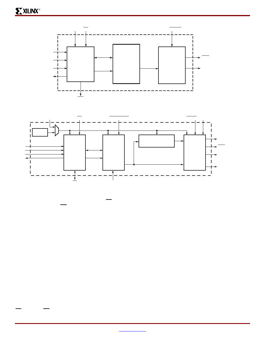
When the FPGA is in Master Serial mode, it generates a
configuration clock that drives the PROM. With CF High, a
short access time after CE and OE are enabled, data is
available on the PROM DATA (D0) pin that is connected to
the FPGA DIN pin. New data is available a short access
time after each rising clock edge. The FPGA generates the
appropriate number of clock pulses to complete the
configuration.
When the FPGA is in Slave Serial mode, the PROM and the
FPGA are both clocked by an external clock source, or
optionally, for the XCFxxP PROM only, the PROM can be
used to drive the FPGA’s configuration clock.
The XCFxxP version of the Platform Flash PROM also
supports Master SelectMAP and Slave SelectMAP (or
Slave Parallel) FPGA configuration modes. When the FPGA
is in Master SelectMAP mode, the FPGA generates a
configuration clock that drives the PROM. When the FPGA
is in Slave SelectMAP Mode, either an external oscillator
generates the configuration clock that drives the PROM and
the FPGA, or optionally, the XCFxxP PROM can be used to
drive the FPGA’s configuration clock. With BUSY Low and
CF High, after CE and OE are enabled, data is available on
the PROMs DATA (D0-D7) pins. New data is available a
short access time after each rising clock edge. The data is
clocked into the FPGA on the following rising edge of the
CCLK. A free-running oscillator can be used in the Slave
Parallel/Slave SelectMAP mode.
The XCFxxP version of the Platform Flash PROM provides
additional advanced features. A built-in data decompressor
supports utilizing compressed PROM files, and design
revisioning allows multiple design revisions to be stored on
a single PROM or stored across several PROMs. For design
revisioning, external pins or internal control bits are used to
select the active design revision.
Multiple Platform Flash PROM devices can be cascaded to
support the larger configuration files required when
targeting larger FPGA devices or targeting multiple FPGAs
daisy chained together. When utilizing the advanced
features for the XCFxxP Platform Flash PROM, such as
design revisioning, programming files which span cascaded
PROM devices can only be created for cascaded chains
containing only XCFxxP PROMs. If the advanced XCFxxP
features are not enabled, then the cascaded chain can
include both XCFxxP and XCFxxS PROMs.
X-Ref Target - Figure 1
Figure 1: XCFxxS Platform Flash PROM Block Diagram
X-Ref Target - Figure 2FI
Figure 2: XCFxxP Platform Flash PROM Block Diagram
Control
and
JTAG
Interface
Memory
Serial
Interface
DATA (D0)
Serial Mode
Data
Address
CLK
CE
TCK
TMS
TDI
TDO
OE/RESET
CEO
Data
ds123_01_30603
CF
CLKOUT
CEO
DATA (D0)
(Serial/Parallel Mode)
D[1:7]
(Parallel Mode)
TCK
TMS
TDI
TDO
CLK
CE
EN_EXT_SEL
OE/RESET
BUSY
Data
Address
REV_SEL [1:0]
CF
Control
and
JTAG
Interface
Memory
OSC
Serial
or
Parallel
Interface
Decompressor
DS123_19_031908
相关PDF资料 |
PDF描述 |
|---|---|
| VI-24Y-CV | CONVERTER MOD DC/DC 3.3V 99W |
| RMC07DREN-S13 | CONN EDGECARD 14POS .100 EXTEND |
| VI-J2M-CY-B1 | CONVERTER MOD DC/DC 10V 50W |
| XC18V01PCG20C | IC PROM SERIAL CONFIG 1M 20-PLCC |
| VI-23Z-CV | CONVERTER MOD DC/DC 2V 60W |
相关代理商/技术参数 |
参数描述 |
|---|---|
| XCF32PVOG48C0936 | 制造商:Xilinx 功能描述:XLXXCF32PVOG48C0936 PROM |
| XCF32PVOG48C4118 | 制造商:Xilinx 功能描述: |
| XCF3-81 | 制造商:SAIA - BURGESS ELECTRONICS INC. 功能描述:Catalogue / XCF3-81 |
| XCF3-81-J1 | 制造商:SAIA - BURGESS ELECTRONICS INC. 功能描述:Catalogue / XCF3-81-J1 |
| XCF3-81-J1Z1 | 制造商:SAIA - BURGESS ELECTRONICS INC. 功能描述:Catalogue / XCF3-81-J1Z1 |
发布紧急采购,3分钟左右您将得到回复。