参数资料
| 型号: | XCS20-3VQ100C |
| 厂商: | Xilinx Inc |
| 文件页数: | 57/83页 |
| 文件大小: | 0K |
| 描述: | IC FPGA 5V C-TEMP 100-VQFP |
| 产品变化通告: | Spartan,Virtex FPGA/SCD Discontinuation 18/Oct/2010 |
| 标准包装: | 90 |
| 系列: | Spartan® |
| LAB/CLB数: | 400 |
| 逻辑元件/单元数: | 950 |
| RAM 位总计: | 12800 |
| 输入/输出数: | 77 |
| 门数: | 20000 |
| 电源电压: | 4.75 V ~ 5.25 V |
| 安装类型: | 表面贴装 |
| 工作温度: | 0°C ~ 85°C |
| 封装/外壳: | 100-TQFP |
| 供应商设备封装: | 100-VQFP(14x14) |
第1页第2页第3页第4页第5页第6页第7页第8页第9页第10页第11页第12页第13页第14页第15页第16页第17页第18页第19页第20页第21页第22页第23页第24页第25页第26页第27页第28页第29页第30页第31页第32页第33页第34页第35页第36页第37页第38页第39页第40页第41页第42页第43页第44页第45页第46页第47页第48页第49页第50页第51页第52页第53页第54页第55页第56页当前第57页第58页第59页第60页第61页第62页第63页第64页第65页第66页第67页第68页第69页第70页第71页第72页第73页第74页第75页第76页第77页第78页第79页第80页第81页第82页第83页
Spartan and Spartan-XL FPGA Families Data Sheet
60
DS060 (v2.0) March 1, 2013
Product Specification
R
Product Obsolete/Under Obsolescence
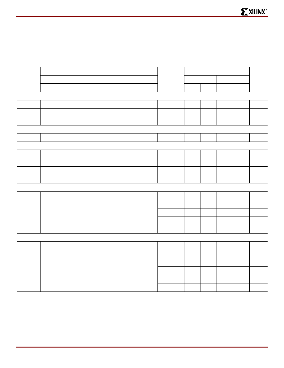
Spartan-XL Family IOB Input Switching Characteristic Guidelines
All devices are 100% functionally tested. Internal timing
parameters are derived from measuring internal test pat-
terns. Listed below are representative values. For more
specific, more precise, and worst-case guaranteed data,
use the values reported by the static timing analyzer (TRCE
in the Xilinx Development System) and back-annotated to
the simulation netlist. These path delays, provided as a
guideline, have been extracted from the static timing ana-
lyzer report. All timing parameters assume worst-case oper-
ating conditions (supply voltage and junction temperature).
Symbol
Device
Speed Grade
Units
-5
-4
Description
Min
Max
Min
Max
Setup Times
TECIK
Clock Enable (EC) to Clock (IK)
All devices
0.0
-
0.0
-
ns
TPICK
Pad to Clock (IK), no delay
All devices
1.0
-
1.2
-
ns
TPOCK
Pad to Fast Capture Latch Enable (OK), no delay
All devices
0.7
-
0.8
-
ns
Hold Times
All Hold Times
All devices
0.0
-
0.0
-
ns
Propagation Delays
TPID
Pad to I1, I2
All devices
-
0.9
-
1.1
ns
TPLI
Pad to I1, I2 via transparent input latch, no delay
All devices
-
2.1
-
2.5
ns
TIKRI
Clock (IK) to I1, I2 (flip-flop)
All devices
-
1.0
-
1.1
ns
TIKLI
Clock (IK) to I1, I2 (latch enable, active Low)
All devices
-
1.1
-
1.2
ns
Delay Adder for Input with Full Delay Option
TDelay
TPICKD = TPICK + TDelay
TPDLI = TPLI + TDelay
XCS05XL
4.0
-
4.7
-
ns
XCS10XL
4.8
-
5.6
-
ns
XCS20XL
5.0
-
5.9
-
ns
XCS30XL
5.5
-
6.5
-
ns
XCS40XL
6.5
-
7.6
-
ns
Global Set/Reset
TMRW
Minimum GSR pulse width
All devices
10.5
-
11.5
-
ns
TRRI
Delay from GSR input to any Q
XCS05XL
-
9.0
-
10.5
ns
XCS10XL
-
9.5
-
11.0
ns
XCS20XL
-
10.0
-
11.5
ns
XCS30XL
-
11.0
-
12.5
ns
XCS40XL
-
12.0
-
13.5
ns
Notes:
1.
Input pad setup and hold times are specified with respect to the internal clock (IK). For setup and hold times with respect to the clock
input, see the pin-to-pin parameters in the Pin-to-Pin Input Parameters table.
2.
Voltage levels of unused pads, bonded or unbonded, must be valid logic levels. Each can be configured with the internal pull-up
(default) or pull-down resistor, or configured as a driven output, or can be driven from an external source.
相关PDF资料 |
PDF描述 |
|---|---|
| XCS20-3TQ144I | IC FPGA 5V I-TEMP 144-TQFP |
| IDT70V05S15J | IC SRAM 64KBIT 15NS 68PLCC |
| MPC8378VRALG | MPU POWERQUICC II PRO 689-PBGA |
| MPC8377VRALG | MPU POWERQUICC II PRO 689-PBGA |
| MPC866PCZP100A | IC MPU POWERQUICC 100MHZ 357PBGA |
相关代理商/技术参数 |
参数描述 |
|---|---|
| XCS20-3VQ100I | 制造商:XILINX 制造商全称:XILINX 功能描述:Spartan and Spartan-XL Families Field Programmable Gate Arrays |
| XCS20-3VQ144C | 制造商:XILINX 制造商全称:XILINX 功能描述:Spartan and Spartan-XL Families Field Programmable Gate Arrays |
| XCS20-3VQ144I | 制造商:XILINX 制造商全称:XILINX 功能描述:Spartan and Spartan-XL Families Field Programmable Gate Arrays |
| XCS20-3VQ208C | 制造商:XILINX 制造商全称:XILINX 功能描述:Spartan and Spartan-XL Families Field Programmable Gate Arrays |
| XCS20-3VQ208I | 制造商:XILINX 制造商全称:XILINX 功能描述:Spartan and Spartan-XL Families Field Programmable Gate Arrays |
发布紧急采购,3分钟左右您将得到回复。