参数资料
| 型号: | XCV200E-8BG352C |
| 厂商: | Xilinx Inc |
| 文件页数: | 183/233页 |
| 文件大小: | 0K |
| 描述: | IC FPGA 1.8V C-TEMP 352-MBGA |
| 产品变化通告: | FPGA Family Discontinuation 18/Apr/2011 |
| 标准包装: | 24 |
| 系列: | Virtex®-E |
| LAB/CLB数: | 1176 |
| 逻辑元件/单元数: | 5292 |
| RAM 位总计: | 114688 |
| 输入/输出数: | 260 |
| 门数: | 306393 |
| 电源电压: | 1.71 V ~ 1.89 V |
| 安装类型: | 表面贴装 |
| 工作温度: | 0°C ~ 85°C |
| 封装/外壳: | 352-LBGA,金属 |
| 供应商设备封装: | 352-MBGA(35x35) |
第1页第2页第3页第4页第5页第6页第7页第8页第9页第10页第11页第12页第13页第14页第15页第16页第17页第18页第19页第20页第21页第22页第23页第24页第25页第26页第27页第28页第29页第30页第31页第32页第33页第34页第35页第36页第37页第38页第39页第40页第41页第42页第43页第44页第45页第46页第47页第48页第49页第50页第51页第52页第53页第54页第55页第56页第57页第58页第59页第60页第61页第62页第63页第64页第65页第66页第67页第68页第69页第70页第71页第72页第73页第74页第75页第76页第77页第78页第79页第80页第81页第82页第83页第84页第85页第86页第87页第88页第89页第90页第91页第92页第93页第94页第95页第96页第97页第98页第99页第100页第101页第102页第103页第104页第105页第106页第107页第108页第109页第110页第111页第112页第113页第114页第115页第116页第117页第118页第119页第120页第121页第122页第123页第124页第125页第126页第127页第128页第129页第130页第131页第132页第133页第134页第135页第136页第137页第138页第139页第140页第141页第142页第143页第144页第145页第146页第147页第148页第149页第150页第151页第152页第153页第154页第155页第156页第157页第158页第159页第160页第161页第162页第163页第164页第165页第166页第167页第168页第169页第170页第171页第172页第173页第174页第175页第176页第177页第178页第179页第180页第181页第182页当前第183页第184页第185页第186页第187页第188页第189页第190页第191页第192页第193页第194页第195页第196页第197页第198页第199页第200页第201页第202页第203页第204页第205页第206页第207页第208页第209页第210页第211页第212页第213页第214页第215页第216页第217页第218页第219页第220页第221页第222页第223页第224页第225页第226页第227页第228页第229页第230页第231页第232页第233页
Virtex-E 1.8 V Field Programmable Gate Arrays
R
DS022-2 (v3.0) March 21, 2014
Module 2 of 4
Production Product Specification
47
— OBSOLETE — OBSOLETE — OBSOLETE — OBSOLETE —
Termination Resistor Packs
Resistor packs are available with the values and the config-
uration required for LVDS and LVPECL termination from
Bourns, Inc., as listed in Table. For pricing and availability,
please contact Bourns directly at http://www.bourns.com
.
LVDS Design Guide
The SelectI/O library elements have been expanded for Vir-
tex-E devices to include new LVDS variants. At this time all
of the cells might not be included in the Synthesis libraries.
The 2.1i-Service Pack 2 update for Alliance and Foundation
software includes these cells in the VHDL and Verilog librar-
ies. It is necessary to combine these cells to create the
P-side (positive) and N-side (negative) as described in the
input, output, 3-state and bidirectional sections.
Creating LVDS Global Clock Input Buffers
Global clock input buffers can be combined with adjacent
IOBs to form LVDS clock input buffers. P-side is the GCLK-
PAD location; N-side is the adjacent IO_LVDS_DLL site.
HDL Instantiation
Only one global clock input buffer is required to be instanti-
ated in the design and placed on the correct GCLKPAD
location. The N-side of the buffer is reserved and no other
IOB is allowed to be placed on this location.
In the physical device, a configuration option is enabled that
routes the pad wire to the differential input buffer located in
the GCLKIOB. The output of this buffer then drives the out-
put of the GCLKIOB cell. In EPIC it appears that the second
buffer is unused. Any attempt to use this location for another
purpose leads to a DRC error in the software.
VHDL Instantiation
gclk0_p : IBUFG_LVDS port map
(I=>clk_external, O=>clk_internal);
Verilog Instantiation
IBUFG_LVDS gclk0_p (.I(clk_external),
.O(clk_internal));
Location constraints
All LVDS buffers must be explicitly placed on a device. For
the global clock input buffers this can be done with the fol-
lowing constraint in the .ucf or .ncf file.
NET clk_external LOC = GCLKPAD3;
GCLKPAD3 can also be replaced with the package pin
name such as D17 for the BG432 package.
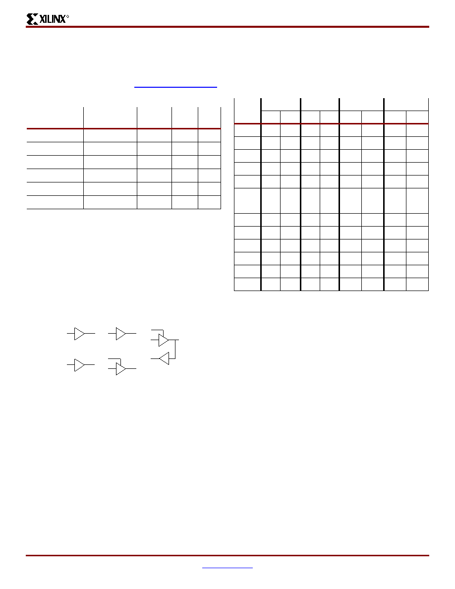
Table 40: Bourns LVDS/LVPECL Resistor Packs
Part Number
I/O Standard
Term.
for:
Pairs/
Pack
Pins
CAT16
LV2F6
LVDS
Driver
2
8
CAT16
LV4F12
LVDS
Driver
4
16
CAT16
PC2F6
LVPECL
Driver
2
8
CAT16
PC4F12
LVPECL
Driver
4
16
CAT16
PT2F2
LVDS/LVPECL
Receiver
2
8
CAT16
PT4F4
LVDS/LVPECL
Receiver
4
16
Figure 58: LVDS elements
O
I
IBUF_LVDS
O
I
OBUF_LVDS
IOBUF_LVDS
O
T
I
OBUFT_LVDS
O
I
IBUFG_LVDS
IO
T
I
x133_22_122299
Table 41: Global Clock Input Buffer Pair Locations
Pkg
GCLK 3
GCLK 2
GCLK 1
GCLK 0
PN
P
N
P
N
P
N
CS144
A6
C6
A7
B7
M7
M6
K7
N8
PQ240
P213
P215
P210 P209
P89
P87
P92
P93
HQ240
P213
P215
P210 P209
P89
P87
P92
P93
BG352
D14
A15
B14
A13
AF14
AD14
AE13
AC13
BG432
D17
C17
A16
B16
AK16
AL17
AL16
AH15
BG560
A17
C18
D17
E17
AJ17
AM18
AL17
AM17
FG256
B8
A7
C9
A8
R8
T8
N8
N9
FG456
C11
B11
A11
D11
Yll
AA11
W12
U12
FG676
E13
B13
C13
F14
AB13
AF13
AA14
AC14
FG680
A20
C22
D21
A19
AU22
AT22
AW19
AT21
FG860
C22
A22
B22
D22
AY22
AW21
BA22
AW20
FG900
C15
A15
E15
E16
AK16
AH16
AJ16
AF16
FG1156
E17
C17
D17
J18
Al19
AL17
AH18
AM18
相关PDF资料 |
PDF描述 |
|---|---|
| SST39VF802C-70-4C-MAQE-T | IC MPF FLASH 8MBIT CMOS 48WFBGA |
| XC4VFX12-11FF668I | IC FPGA VIRTEX-4FX 668FFBGA |
| XC4VFX12-12FFG668C | IC FPGA VIRTEX-4 FX 12K 668FCBGA |
| SST39VF801C-70-4I-MAQE-T | IC MPF FLASH 8MBIT CMOS 48WFBGA |
| XC4VFX12-11FFG668I | IC FPGA VIRTEX-4 FX 12K 668FCBGA |
相关代理商/技术参数 |
参数描述 |
|---|---|
| XCV200E-8BG352I | 制造商:XILINX 制造商全称:XILINX 功能描述:Virtex-E 1.8 V Field Programmable Gate Arrays |
| XCV200E-8CS144C | 功能描述:IC FPGA 1.8V C-TEMP 144-CSBGA RoHS:否 类别:集成电路 (IC) >> 嵌入式 - FPGA(现场可编程门阵列) 系列:Virtex®-E 产品变化通告:Step Intro and Pkg Change 11/March/2008 标准包装:1 系列:Virtex®-5 SXT LAB/CLB数:4080 逻辑元件/单元数:52224 RAM 位总计:4866048 输入/输出数:480 门数:- 电源电压:0.95 V ~ 1.05 V 安装类型:表面贴装 工作温度:-40°C ~ 100°C 封装/外壳:1136-BBGA,FCBGA 供应商设备封装:1136-FCBGA 配用:568-5088-ND - BOARD DEMO DAC1408D750122-1796-ND - EVALUATION PLATFORM VIRTEX-5 |
| XCV200E-8CS144I | 制造商:XILINX 制造商全称:XILINX 功能描述:Virtex-E 1.8 V Field Programmable Gate Arrays |
| XCV200E-8FG240C | 制造商:XILINX 制造商全称:XILINX 功能描述:Virtex⑩-E 1.8 V Field Programmable Gate Arrays |
| XCV200E-8FG240I | 制造商:XILINX 制造商全称:XILINX 功能描述:Virtex⑩-E 1.8 V Field Programmable Gate Arrays |
发布紧急采购,3分钟左右您将得到回复。