- 您现在的位置:买卖IC网 > PDF目录277731 > XD-14590D5-422L (DATA DEVICE CORP) SYNCHRO OR RESOLVER TO DIGITAL CONVERTER, MDMA36 PDF资料下载
参数资料
| 型号: | XD-14590D5-422L |
| 厂商: | DATA DEVICE CORP |
| 元件分类: | 位置变换器 |
| 英文描述: | SYNCHRO OR RESOLVER TO DIGITAL CONVERTER, MDMA36 |
| 封装: | DDIP-36 |
| 文件页数: | 13/16页 |
| 文件大小: | 150K |
| 代理商: | XD-14590D5-422L |
6
Data Device Corporation
www.ddc-web.com
SD-14590/91/92
D-02/02-250
DIGITAL INTERFACE
The digital interface circuitry has three main functions: to latch
the output bits during an inhibit command so that the stable data
can be read; to furnish both parallel and three-state data formats;
and to act as a buffer between the internal CMOS logic and the
external TTL logic.
In the SD-14590, applying an inhibit command will lock the data
in the transparent latch without interfering with the continuous
tracking of the feedback loop. Therefore, the digital angle is
always updated, and the inhibit can be applied for an arbitrary
amount of time. The inhibit transparent latch and the 50 ns delay
are part of the inhibit circuitry. The inhibit circuitry is described in
detail in the logic input/output section.
LOGIC INPUT/OUTPUT
Logic angle outputs consist of 14 or 16 parallel data bits and
CONVERTER BUSY (CB). All logic outputs are short-circuit
proof to ground and +5 Volts. The CB output is a positive, 0.4 to
2.0 s pulse. Data changes about 50 ns after the leading edge of
the pulse because of an internal delay. Data is valid 0.2 s after
the leading edge of CB, the angle is determined by the sum of
the bits at logic “1.” Digital outputs are three-state and two bytes
wide. For 14 bit only: 1-6 (MSB’s) are enabled by signal EM, bits
7-14 (LSB’s) are enabled by the signal EL; for 14/16 program-
mable: 1-8 (MSB’s) are enabled by signal EM, 9-14 (LSB’s 14 bit)
or 9-16 (LSB’s 16 bit) are enabled by the signal EL. Outputs are
valid (logic “1” or “0”) 150 ns max after setting EM or EL low, and
are high impedance within 100 ns max of setting EM or EL high.
Both EM and EL are internally pulled-down to +5 V at 30 A max.
The inhibit (INH) input locks the transparent latch so the bits will
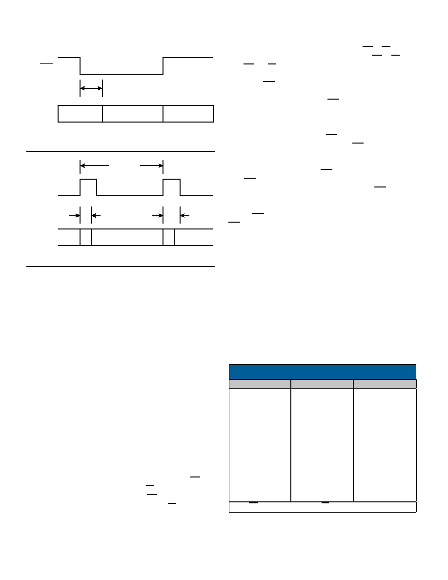
remain stable while data is being transferred (See FIGURE 1).
The output is stable 0.5 s after INH is driven to logic “0,” see
FIGURE 4. A logic “0” at the T input latches the data, and a logic
“1” applied to T will allow the bits to change. The inhibit trans-
parent latch prevents the transmission of invalid data when there
is an overlap between CB and INH. While the counter is not
being updated, CB is at logic “0” and the INH latch is transpar-
ent.
When CB goes to logic “1,” the INH latch is locked. If CB occurs
after INH has been applied, the latch will remain locked and its
data will not change until CB returns to logic “0.” If INH is applied
during CB, the latch will not lock until the CB pulse is over. The
purpose of the 50 ns delay is to prevent a race condition between
CB and INH where the up-down counter begins to change as an
INH is applied. Whenever an input angle change occurs, the
converter changes the digital angle in 1 LSB steps and gener-
ates a converter busy pulse. Output data change is initiated by
the leading edge of the CB pulse, delayed by 50 ns, nominal.
Valid data is available at the outputs 0.2 s after the leading
edge of CB, see FIGURE 5.
RESOLUTION CONTROL
Resolution control is via one logic input A. The SD-14590 (not
the SD-14591 or SD-14592) has programmable resolution.
BUILT-IN-TEST
The Built-ln-Test output (BIT) monitors the level of error (D) from
the demodulator. D represents the difference in the input and
output angles and ideally should be zero. If it exceeds approxi-
;;
DATA
VALID
0.5
s
ASYNCHRONOUS TO CB
INH
FIGURE 4. INHIBIT TIMING DIAGRAM
;
DEPENDS ON d
φ/dt
0.4-2.0
s
CB
0.2
s
DATA
VALID
6.1
s MIN
FIGURE 5. CONVERTER BUSY TIMING DIAGRAM
MIN/BIT
BIT
DEG/BIT
TABLE 2. DIGITAL ANGLE OUTPUTS
1 MSB
2
3
4
5
6
7
8
9
10
11
12
13
14
15
16
180
90
45
22.5
11.25
5.625
2.813
1.405
0.7031
0.3516
0.1758
0.0879
0.0439
0.0220
0.0110
0.0055
10,800
5,400
2,700
1,350
675
387.5
168.75
84.38
42.19
21.09
10.55
5.27
2.64
1.32
0.66
0.33
Note: EM enables the MSB’s and EL enables the LSB’s.
相关PDF资料 |
PDF描述 |
|---|---|
| XD-14595D5-504S | SYNCHRO OR RESOLVER TO DIGITAL CONVERTER, DIP36 |
| XD-14595D5-532K | SYNCHRO OR RESOLVER TO DIGITAL CONVERTER, DIP36 |
| XMRA104S-F-4F700 | 104 CONTACT(S), FEMALE, MULTIWAY RACK AND PANEL CONN, SOLDER, RECEPTACLE |
| XMRA104S-F-4F710 | 104 CONTACT(S), FEMALE, MULTIWAY RACK AND PANEL CONN, SOLDER, RECEPTACLE |
| XMRA104S-F-4F800 | 104 CONTACT(S), FEMALE, MULTIWAY RACK AND PANEL CONN, SOLDER, RECEPTACLE |
相关代理商/技术参数 |
参数描述 |
|---|---|
| XD-14595D4-102 | 制造商:未知厂家 制造商全称:未知厂家 功能描述:Resolver/Synchro-to-Digital Converter |
| XD-14595D4-104 | 制造商:未知厂家 制造商全称:未知厂家 功能描述:Resolver/Synchro-to-Digital Converter |
| XD-14595D4-105 | 制造商:未知厂家 制造商全称:未知厂家 功能描述:Resolver/Synchro-to-Digital Converter |
| XD-14595D4-112 | 制造商:未知厂家 制造商全称:未知厂家 功能描述:Resolver/Synchro-to-Digital Converter |
| XD-14595D4-114 | 制造商:未知厂家 制造商全称:未知厂家 功能描述:Resolver/Synchro-to-Digital Converter |
发布紧急采购,3分钟左右您将得到回复。