- 您现在的位置:买卖IC网 > PDF目录277731 > XD-14590D5-422L (DATA DEVICE CORP) SYNCHRO OR RESOLVER TO DIGITAL CONVERTER, MDMA36 PDF资料下载
参数资料
| 型号: | XD-14590D5-422L |
| 厂商: | DATA DEVICE CORP |
| 元件分类: | 位置变换器 |
| 英文描述: | SYNCHRO OR RESOLVER TO DIGITAL CONVERTER, MDMA36 |
| 封装: | DDIP-36 |
| 文件页数: | 14/16页 |
| 文件大小: | 150K |
| 代理商: | XD-14590D5-422L |
7
Data Device Corporation
www.ddc-web.com
SD-14590/91/92
D-02/02-250
ERROR PROCESSOR
INPUT
θ
Open Loop Transfer function = Output
WHERE:
2
A = A A
1
2
VELOCITY
OUT
DIGITAL
POSITION
OUT
(
φ)
VCO
CT
S
A
+ 1
1
B
S
+ 1
10B
H = 1
2
S
A
+ 1
B
2
S
+ 1
10B
+
-
e
A
2
S
2.75
FIGURE 6. CONTROL LOOP BLOCK DIAGRAM
-12
db/oct
4
BA
(BW)
2A
-6 db/oct
10B
ω (rad/sec)
FIGURE 7. OPEN LOOP BODE PLOT
BANDWIDTH
PARAMETER
UNITS
TABLE 3. DYNAMIC CHARACTERISTICS
RESOLUTION
Input Frequency
Tracking Rate
Bandwidth
Ka
A1
A2
A
B
acc-1 LSB lag
Settling Time
BITS
Hertz
RPS min
Hertz
1/sec2 nom
1/sec nom
Deg/sec2 nom
ms max
14
16
360 - 1000
10
2.5
54
*
12500
*
0.31
*
40k
*
112
*
52
*
275k
69
300
800
Note: * means the same as value to the left.
400 HZ
60 HZ
14
16
47 - 1000
2.5
0.61
14
*
780
*
0.078
*
10k
*
28
*
13
*
17
4.3
1400
3400
BIT will also be set if a total Loss-of-Signal (LOS) and/or a Loss-
of-Reference (LOR) occurs.
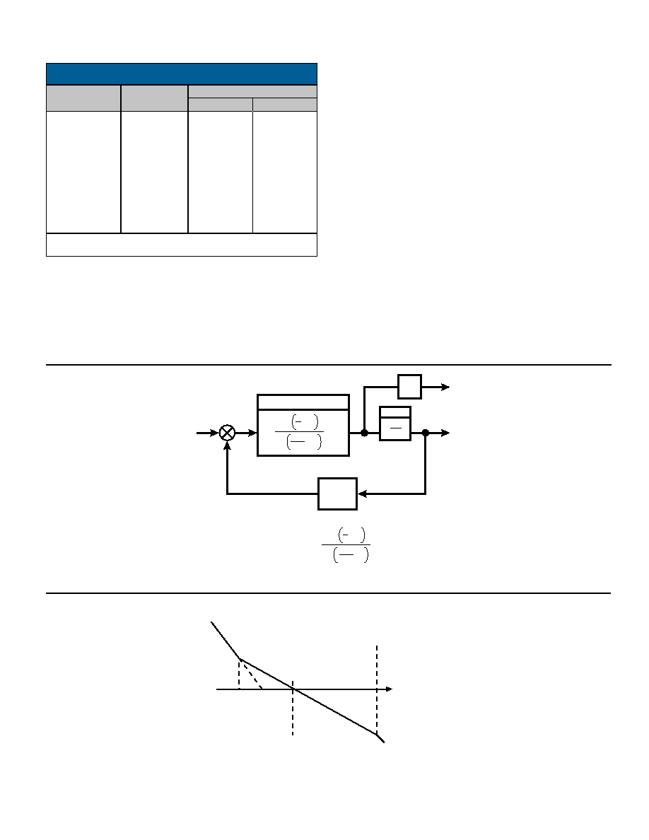
DYNAMIC PERFORMANCE
A Type II servo loop (Kv =
∞) and very high acceleration con-
stants give the SD-14590 superior dynamic performance, as list-
ed in TABLE 3. If the power supply voltages are not the ±15 VDC
nominal values, the specified input rates will increase or
decrease in proportion to the fractional change in voltage. A
Control Loop Block Diagram is shown in FIGURE 6, and an
Open Loop Bode Plot is shown in FIGURE 7. The values of the
transfer function coefficients are shown in TABLE 3.
An inhibit input, regardless of its duration, does not affect the
converter update. A simple method of interfacing to a computer
asynchronously to CB is: (A) apply the inhibit, (B) wait 0.5 s
minimum, (C) transfer the data and (D) release the inhibit.
As long as the converter maximum tracking rate is not exceed-
ed, there will be no lag in the converter output. If a step input
occurs, as when the power is initially applied, the response will
mately 65 LSBs (of the selected resolution), the logic level at BIT
will change from a logic 0 to logic 1. This condition will occur dur-
ing a large step and reset after the converter settles out. BIT will
also change to logic 1 for an over-velocity condition, because the
converter loop cannot maintain input-output and/or if the con-
verter malfunctions where it cannot maintain the loop at a null.
相关PDF资料 |
PDF描述 |
|---|---|
| XD-14595D5-504S | SYNCHRO OR RESOLVER TO DIGITAL CONVERTER, DIP36 |
| XD-14595D5-532K | SYNCHRO OR RESOLVER TO DIGITAL CONVERTER, DIP36 |
| XMRA104S-F-4F700 | 104 CONTACT(S), FEMALE, MULTIWAY RACK AND PANEL CONN, SOLDER, RECEPTACLE |
| XMRA104S-F-4F710 | 104 CONTACT(S), FEMALE, MULTIWAY RACK AND PANEL CONN, SOLDER, RECEPTACLE |
| XMRA104S-F-4F800 | 104 CONTACT(S), FEMALE, MULTIWAY RACK AND PANEL CONN, SOLDER, RECEPTACLE |
相关代理商/技术参数 |
参数描述 |
|---|---|
| XD-14595D4-102 | 制造商:未知厂家 制造商全称:未知厂家 功能描述:Resolver/Synchro-to-Digital Converter |
| XD-14595D4-104 | 制造商:未知厂家 制造商全称:未知厂家 功能描述:Resolver/Synchro-to-Digital Converter |
| XD-14595D4-105 | 制造商:未知厂家 制造商全称:未知厂家 功能描述:Resolver/Synchro-to-Digital Converter |
| XD-14595D4-112 | 制造商:未知厂家 制造商全称:未知厂家 功能描述:Resolver/Synchro-to-Digital Converter |
| XD-14595D4-114 | 制造商:未知厂家 制造商全称:未知厂家 功能描述:Resolver/Synchro-to-Digital Converter |
发布紧急采购,3分钟左右您将得到回复。