参数资料
| 型号: | XE8802MI035LF |
| 厂商: | Semtech |
| 文件页数: | 36/193页 |
| 文件大小: | 0K |
| 描述: | IC DAS 16BIT FLASH 8K 100-LQFP |
| 标准包装: | 90 |
| 系列: | XE880x |
| 应用: | 感测机 |
| 核心处理器: | Coolrisc816? |
| 程序存储器类型: | 闪存(22 kB) |
| 控制器系列: | XE8000 |
| RAM 容量: | 1K x 8 |
| 接口: | SPI,UART |
| 输入/输出数: | 36 |
| 电源电压: | 2.4 V ~ 5.5 V |
| 工作温度: | -40°C ~ 85°C |
| 安装类型: | 表面贴装 |
| 封装/外壳: | 100-LQFP |
| 包装: | 托盘 |
| 供应商设备封装: | 100-LQFP(14x14) |
| 产品目录页面: | 585 (CN2011-ZH PDF) |
| 配用: | XE8000MP-ND - PROG BOARD AND PROSTART2 CARD |
第1页第2页第3页第4页第5页第6页第7页第8页第9页第10页第11页第12页第13页第14页第15页第16页第17页第18页第19页第20页第21页第22页第23页第24页第25页第26页第27页第28页第29页第30页第31页第32页第33页第34页第35页当前第36页第37页第38页第39页第40页第41页第42页第43页第44页第45页第46页第47页第48页第49页第50页第51页第52页第53页第54页第55页第56页第57页第58页第59页第60页第61页第62页第63页第64页第65页第66页第67页第68页第69页第70页第71页第72页第73页第74页第75页第76页第77页第78页第79页第80页第81页第82页第83页第84页第85页第86页第87页第88页第89页第90页第91页第92页第93页第94页第95页第96页第97页第98页第99页第100页第101页第102页第103页第104页第105页第106页第107页第108页第109页第110页第111页第112页第113页第114页第115页第116页第117页第118页第119页第120页第121页第122页第123页第124页第125页第126页第127页第128页第129页第130页第131页第132页第133页第134页第135页第136页第137页第138页第139页第140页第141页第142页第143页第144页第145页第146页第147页第148页第149页第150页第151页第152页第153页第154页第155页第156页第157页第158页第159页第160页第161页第162页第163页第164页第165页第166页第167页第168页第169页第170页第171页第172页第173页第174页第175页第176页第177页第178页第179页第180页第181页第182页第183页第184页第185页第186页第187页第188页第189页第190页第191页第192页第193页
Semtech 2006
www.semtech.com
17-18
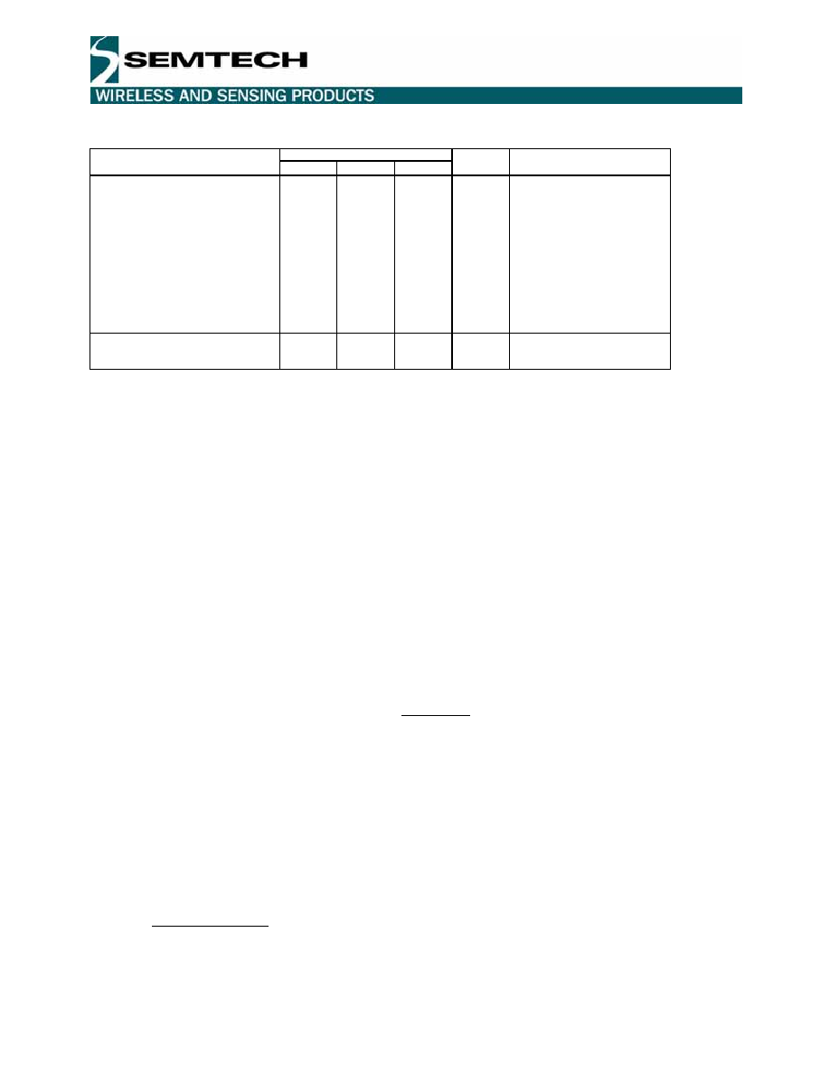
XE8802 Sensing Machine Data Acquisition MCU
with ZoomingADC and LCD driver
Specifications (Cont’d)
VALUE
PARAMETER
MIN
TYP
MAX
UNITS
COMMENTS/CONDITIONS
POWER SUPPLY
Voltage Supply Range, VDD
Analog
Quiescent
Current
Consumption, Total (IQ)
ADC Only
PGA1
PGA2
PGA3
Analog Power Dissipation
Normal Power Mode
3/4 Power Reduction Mode
1/2 Power Reduction Mode
1/4 Power Reduction Mode
+2.4
+5
720/620
250/190
165/150
130/120
175/160
3.6/1.9
2.7/1.4
1.8/0.9
0.9/0.5
+5.5
V
A
mW
Only Acquisition Chain
VDD = 5V/3V
All PGAs & ADC Active
VDD = 5V/3V (Note 16)
VDD = 5V/3V (Note 17)
VDD = 5V/3V (Note 18)
VDD = 5V/3V (Note 19)
TEMPERATURE
Specified Range
Operating Range
-40
+85
+125
°C
Notes:
(1)
Gain
defined
as
overall
PGA
gain
GDTOT
=
GD1GD2GD3.
Maximum
input
voltage
is
given
by:
VIN,MAX = ±(VREF/2)(OSR/OSR+1).
(2)
Offset due to tolerance on GDoff2 or GDoff3 setting. For small intrinsic offset, use only ADC and PGA1.
(3)
Measured with block connected to inputs through AMUX block. Normalized input sampling frequency for input impedance is fS =
512kHz. This figure must be multiplied by 2 for fS = 256kHz, 4 for fS = 128kHz. Input impedance is proportional to 1/fS.
(4)
Figure
independent
from
PGA1
gain
and
sampling
frequency
fS.
See
model
of
Figure
17-18(a).
See equation Eq. 21 to calculate equivalent input noise.
(5)
Figure independent on PGA2 gain and sampling frequency fS. See model of Figure 17-18(a). See equation Eq. 21 to calculate
equivalent input noise.
(6)
Figure independent on PGA3 gain and sampling frequency fS. See model of Figure 17-18(a) and equation Eq. 21 to calculate
equivalent input noise.
(7)
Resolution is given by n = 2
log2(OSR) + log2(N
ELCONV). OSR can be set between 8 and 1024, in powers of 2. NELCONV can be set to
1, 2, 4 or 8.
(8)
If a ramp signal is applied to the input, all digital codes appear in the resulting ADC output data.
(9)
Gain error is defined as the amount of deviation between the ideal (theoretical) transfer function and the measured transfer function
(with the offset error removed). (See Figure 17-19)
(10) Offset error is defined as the output code error for a zero volt input (ideally, output code = 0). For
± 1 LSB offset, N
ELCONV must be ≥2.
(11) INL defined as the deviation of the DC transfer curve of each individual code from the best-fit straight line. This specification holds
over the full scale.
(12) DNL is defined as the difference (in LSB) between the ideal (1 LSB) and measured code transitions for successive codes.
(13) Figures for Gains = 1 to 100. PSRR is defined as the amount of change in the ADC output value as the power supply voltage
changes.
(14) Conversion time is given by: TCONV = (NELCONV (OSR + 1) + 1) / fS. OSR can be set between 8 and 1024, in powers of 2. NELCONV can
be set to 1, 2, 4 or 8.
(15) PGAs are reset after each writing operation to registers RegAcCfg1-5. The ADC must be started after a PGA or inputs common-
mode stabilisation delay. This is done by writing bit Start several cycles after PGA settings modification or channel switching.
Delay between PGA start or input channel switching and ADC start should be equivalent to OSR (between 8 and 1024) number of
cycles. This delay does not apply to conversions made without the PGAs.
(16) Nominal (maximum) bias currents in PGAs and ADC, i.e. IB_AMP_PGA[1:0] = ‘11’ and IB_AMP_ADC[1:0] = ‘11’.
(17) Bias currents in PGAs and ADC set to 3/4 of nominal values, i.e. IB_AMP_PGA[1:0] = ‘10’, IB_AMP_ADC[1:0] = ‘10’.
(18) Bias currents in PGAs and ADC set to 1/2 of nominal values, i.e. IB_AMP_PGA[1:0] = ‘01’, IB_AMP_ADC[1:0] = ‘01’.
(19) Bias currents in PGAs and ADC set to 1/4 of nominal values, i.e. IB_AMP_PGA[1:0] = ‘00’, IB_AMP_ADC[1:0] = ‘00’.
17.8.3
Linearity
17.8.3.1
Integral non-linearity
The integral non-linearity depends on the selected gain configuration. First of all, the non-linearity of the ADC (all
PGA stages bypassed) is shown in Figure 17-8.
Not
Recommended
for
New
Designs
相关PDF资料 |
PDF描述 |
|---|---|
| XE8805AMI028LF | IC DAS 16BIT FLASH 8K MTP 64LQFP |
| XE8807AMI026TLF | IC MCU LOW PWR MTP FLASH 32-TQFP |
| XIO2200AGGW | IC PCI-EXPRESS/BUS BRIDGE 176BGA |
| XIO2200AZGW | IC PCI-EXPRESS/BUS BRIDGE 176BGA |
| XPC823ZT81B2T | IC MPU POWERQUICC 81MHZ 256-PBGA |
相关代理商/技术参数 |
参数描述 |
|---|---|
| XE8805 | 制造商:SEMTECH 制造商全称:Semtech Corporation 功能描述:Data Acquisition MCU |
| XE8805AMI000 | 制造商:SEMTECH 制造商全称:Semtech Corporation 功能描述:Data Acquisition MCU |
| XE8805AMI028LF | 功能描述:IC DAS 16BIT FLASH 8K MTP 64LQFP RoHS:是 类别:集成电路 (IC) >> 嵌入式 - 微控制器 - 特定应用 系列:XE880x 产品变化通告:Product Discontinuation 26/Aug/2009 标准包装:250 系列:- 应用:网络处理器 核心处理器:4Kc 程序存储器类型:- 控制器系列:- RAM 容量:16K x 8 接口:以太网,UART,USB 输入/输出数:- 电源电压:1.8V, 3.3V 工作温度:- 安装类型:表面贴装 封装/外壳:208-LQFP 包装:带卷 (TR) 供应商设备封装:PG-LQFP-208 其它名称:SP000314382 |
| XE8805AMI028TLF | 制造商:Semtech Corporation 功能描述: |
| XE8805MI028 | 制造商:SEMTECH 制造商全称:Semtech Corporation 功能描述:Data Acquisition MCU |
发布紧急采购,3分钟左右您将得到回复。