参数资料
| 型号: | XR16C2550IMTR-F |
| 厂商: | Exar Corporation |
| 文件页数: | 11/37页 |
| 文件大小: | 0K |
| 描述: | IC UART FIFO 16B DUAL 48TQFP |
| 标准包装: | 1,500 |
| 特点: | * |
| 通道数: | 2,DUART |
| FIFO's: | 16 字节 |
| 规程: | RS232,RS485 |
| 电源电压: | 2.97 V ~ 5.5 V |
| 带故障启动位检测功能: | 是 |
| 带调制解调器控制功能: | 是 |
| 带CMOS: | 是 |
| 安装类型: | 表面贴装 |
| 封装/外壳: | 48-TQFP |
| 供应商设备封装: | 48-TQFP(7x7) |
| 包装: | 带卷 (TR) |
第1页第2页第3页第4页第5页第6页第7页第8页第9页第10页当前第11页第12页第13页第14页第15页第16页第17页第18页第19页第20页第21页第22页第23页第24页第25页第26页第27页第28页第29页第30页第31页第32页第33页第34页第35页第36页第37页
XR16C2550
19
REV. 1.0.2
2.97V TO 5.5V DUART WITH 16-BYTE FIFO
4.5
FIFO Control Register (FCR) - Write-Only
This register is used to enable the FIFOs, clear the FIFOs, set the transmit/receive FIFO trigger levels, and
select the DMA mode. The DMA, and FIFO modes are defined as follows:
FCR[0]: TX and RX FIFO Enable
Logic 0 = Disable the transmit and receive FIFO (default).
Logic 1 = Enable the transmit and receive FIFOs. This bit must be set to logic 1 when other FCR bits are
written or they will not be programmed.
FCR[1]: RX FIFO Reset
This bit is only active when FCR bit-0 is a ‘1’.
Logic 0 = No receive FIFO reset (default)
Logic 1 = Reset the receive FIFO pointers (the receive shift register is not cleared or altered). This bit will
return to a logic 0 after resetting the FIFO.
FCR[2]: TX FIFO Reset
This bit is only active when FCR bit-0 is a ‘1’.
Logic 0 = No transmit FIFO reset (default).
Logic 1 = Reset the transmit FIFO pointers (the transmit shift register is not cleared or altered). This bit will
return to a logic 0 after resetting the FIFO.
FCR[3]: DMA Mode Select
Controls the behavior of the TXRDY# and RXRDY# pins. See DMA operation section for details.
Logic 0 = Normal Operation (default).
Logic 1 = DMA Mode.
FCR[5:4]: Reserved
FCR[7:6]: Receive FIFO Trigger Select
(logic 0 = default, RX trigger level =1)
These 2 bits are used to set the trigger level for the receive FIFO. The UART will issue a receive interrupt when
the number of the characters in the FIFO crosses the trigger level. Table 9 shows the complete selections.
4.6
Line Control Register (LCR) - Read/Write
The Line Control Register is used to specify the asynchronous data communication format. The word or
character length, the number of stop bits, and the parity are selected by writing the appropriate bits in this
register.
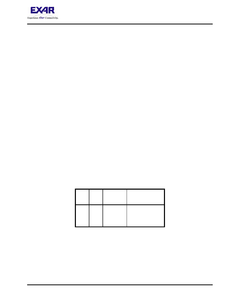
TABLE 9: RECEIVE FIFO TRIGGER LEVEL SELECTION
FCR
BIT-7
FCR
BIT-6
RECEIVE
TRIGGER
LEVEL
COMPATIBILITY
0
1
0
1
0
1
1 (default)
4
8
14
16C550, 16C2552,
16C554, 16C580 com-
patible.
相关PDF资料 |
PDF描述 |
|---|---|
| ST78C34CP40-F | IC UART FIFO 83B 40PDIP |
| XR16M2551IL32TR-F | IC UART FIFO 16B DUAL 32QFN |
| XR16L2551ILTR-F | IC UART FIFO 16B DUAL 32QFN |
| XR16L2750IMTR-F | IC UART FIFO 64B DUAL 48TQFP |
| XR16L2552IJTR-F | IC UART FIFO 16B DUAL 44PLCC |
相关代理商/技术参数 |
参数描述 |
|---|---|
| XR16C2550IP | 制造商:EXAR 制造商全称:EXAR 功能描述:2.97V TO 5.5V DUART WITH 16-BYTE FIFO |
| XR16C2552 | 制造商:EXAR 制造商全称:EXAR 功能描述:2.97V TO 5.5V DUAL UART WITH 16-BYTE FIFO |
| XR16C2552IJ | 制造商:EXAR 制造商全称:EXAR 功能描述:2.97V TO 5.5V DUAL UART WITH 16-BYTE FIFO |
| XR16C2850 | 制造商:EXAR 制造商全称:EXAR 功能描述:2.97V TO 5.5V DUAL UART WITH 128-BYTE FIFOS |
| XR16C2850_05 | 制造商:EXAR 制造商全称:EXAR 功能描述:2.97V TO 5.5V DUAL UART WITH 128-BYTE FIFOS |
发布紧急采购,3分钟左右您将得到回复。