- 您现在的位置:买卖IC网 > PDF目录10739 > XRD98L59AIG (Exar Corporation)IC CCD DIGITIZER 10BIT 28TSSOP PDF资料下载
参数资料
| 型号: | XRD98L59AIG |
| 厂商: | Exar Corporation |
| 文件页数: | 6/37页 |
| 文件大小: | 0K |
| 描述: | IC CCD DIGITIZER 10BIT 28TSSOP |
| 产品变化通告: | Obsolescence Notification 15/Apr/2010 |
| 标准包装: | 50 |
| 位数: | 10 |
| 通道数: | 1 |
| 电压 - 电源,模拟: | 2.7 V ~ 3.6 V |
| 电压 - 电源,数字: | 2.7 V ~ 3.6 V |
| 封装/外壳: | 28-TSSOP(0.173",4.40mm 宽) |
| 供应商设备封装: | 28-TSSOP |
| 包装: | 管件 |
第1页第2页第3页第4页第5页当前第6页第7页第8页第9页第10页第11页第12页第13页第14页第15页第16页第17页第18页第19页第20页第21页第22页第23页第24页第25页第26页第27页第28页第29页第30页第31页第32页第33页第34页第35页第36页第37页
XRD98L59
14
Rev. 2.00
RSTREJ reduces CCD reset noise by disconnecting the
input of the XRD98L59 from the CCD during the CCD
reset pulse. RSTREJ is an internally generated signal.
RSTREJ disconnects the input after the SPIX and before
the SBLK sampling events to reject CCD reset noise.
The RSTREJ switch is always closed (the input is always
connected) if D6=0 in the clock register (address 0011)
of the serial port.
For the timing example shown in Figure 6, SBLK high
samples the pixel black level. The actual hold point of
the pixel black level occurs after a delay of tBK. tBK is
the aperture delay of the SBLK timing signal.
The polarities of the SBLK and SPIX signals are indepen-
dently programmable via the serial port.
For the timing example shown in Figure 6, SPIX high
samples the pixel video level. The actual hold point of
the pixel video level occurs after a delay of tVD. tVD is
the aperture delay of the SPIX timing signal. The
polarity of the SPIX signal is serial port programmable.
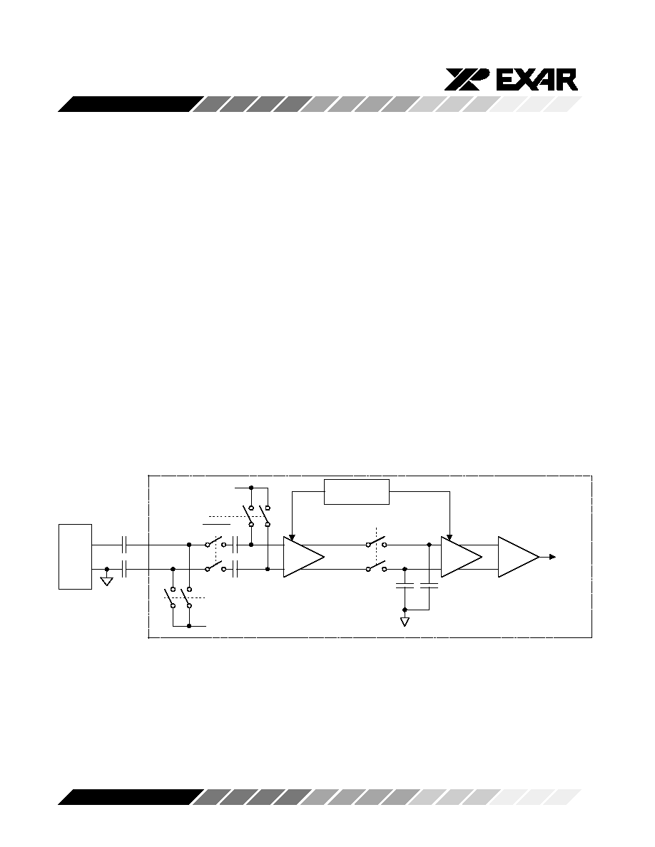
The function of the CDS block, shown in Figure 7, is to
sense the voltage difference between the black level and
video level for each pixel. The CDS and PGA are fully
differential to reject common mode noise. The PGA
output is converted to a single ended signal, and then fed
to the ADC.
REF
IN (CDS non-inverting input) should be connected,
via a capacitor, to the CCD “Common” voltage. This is
typically CCD ground.
CCD
IN (CDS inverting input)
should be connected, via a capacitor, to the CCD output
signal. The external coupling capacitors on CCD
IN and
REF
IN should be of equal values to minimize gain errors
(typically 0.01
f +/-10%).
Figure 7. Block Diagram of the CDS, Reset Phase: RSTREJ Switch is Open
+
PGA1
-
Vbias1 ~0.8
External
Coupling
Capacitors
VBIAS2
CLAMP
φ1
Gain
Register
to ADC
C
D
GND
Vout
C1
C2
C3
+
PGA2
-
+
BUF
-
C4
φ2
RSTREJ
相关PDF资料 |
PDF描述 |
|---|---|
| XRD9827ACDTR-F | IC 12B CCD/CIS SIG PROC 20SOIC |
| XRD9827ACD-F | IC 12B CCD/CIS SIG PROC 20SOIC |
| XRD9826ACU | IC 16B CCD/CIS SIG PROC 20SSOP |
| XRD9826ACD-F | IC 16B CCD/CIS SIG PROC 20SOIC |
| VE-B1J-MY-B1 | CONVERTER MOD DC/DC 36V 50W |
相关代理商/技术参数 |
参数描述 |
|---|---|
| XRD98L59AIG-F | 功能描述:模数转换器 - ADC RoHS:否 制造商:Texas Instruments 通道数量:2 结构:Sigma-Delta 转换速率:125 SPs to 8 KSPs 分辨率:24 bit 输入类型:Differential 信噪比:107 dB 接口类型:SPI 工作电源电压:1.7 V to 3.6 V, 2.7 V to 5.25 V 最大工作温度:+ 85 C 安装风格:SMD/SMT 封装 / 箱体:VQFN-32 |
| XRD98L59AIGTR | 功能描述:模数转换器 - ADC RoHS:否 制造商:Texas Instruments 通道数量:2 结构:Sigma-Delta 转换速率:125 SPs to 8 KSPs 分辨率:24 bit 输入类型:Differential 信噪比:107 dB 接口类型:SPI 工作电源电压:1.7 V to 3.6 V, 2.7 V to 5.25 V 最大工作温度:+ 85 C 安装风格:SMD/SMT 封装 / 箱体:VQFN-32 |
| XRD98L59AIGTR-F | 功能描述:模数转换器 - ADC RoHS:否 制造商:Texas Instruments 通道数量:2 结构:Sigma-Delta 转换速率:125 SPs to 8 KSPs 分辨率:24 bit 输入类型:Differential 信噪比:107 dB 接口类型:SPI 工作电源电压:1.7 V to 3.6 V, 2.7 V to 5.25 V 最大工作温度:+ 85 C 安装风格:SMD/SMT 封装 / 箱体:VQFN-32 |
| XRD98L61 | 制造商:EXAR 制造商全称:EXAR 功能描述:CCD Image Digitizers with CDS, PGA and 12-Bit A/D |
| XRD98L61_01 | 制造商:EXAR 制造商全称:EXAR 功能描述:CCD Image Digitizers with CDS, PGA and 12-Bit A/D |
发布紧急采购,3分钟左右您将得到回复。