参数资料
| 型号: | XRT83L38IB-F |
| 厂商: | Exar Corporation |
| 文件页数: | 68/87页 |
| 文件大小: | 0K |
| 描述: | IC LIU T1/E1/J1 OCTAL 225BGA |
| 标准包装: | 84 |
| 类型: | 线路接口装置(LIU) |
| 驱动器/接收器数: | 8/8 |
| 规程: | T1,E1,J1 |
| 电源电压: | 3.135 V ~ 3.465 V |
| 安装类型: | 表面贴装 |
| 封装/外壳: | 225-BGA |
| 供应商设备封装: | 225-BGA(19x19) |
| 包装: | 托盘 |
第1页第2页第3页第4页第5页第6页第7页第8页第9页第10页第11页第12页第13页第14页第15页第16页第17页第18页第19页第20页第21页第22页第23页第24页第25页第26页第27页第28页第29页第30页第31页第32页第33页第34页第35页第36页第37页第38页第39页第40页第41页第42页第43页第44页第45页第46页第47页第48页第49页第50页第51页第52页第53页第54页第55页第56页第57页第58页第59页第60页第61页第62页第63页第64页第65页第66页第67页当前第68页第69页第70页第71页第72页第73页第74页第75页第76页第77页第78页第79页第80页第81页第82页第83页第84页第85页第86页第87页
XRT83L38
67
OCTAL T1/E1/J1 LH/SH TRANSCEIVER WITH CLOCK RECOVERY AND JITTER ATTENUATOR
REV. 1.0.2
CLOCK SELECT REGISTER
The input clock source is used to generate all the necessary clock references internally to the LIU. The
microprocessor timing is derived from a PLL output which is chosen by programming the Clock Select Bits and
the Master Clock Rate in register 0x81h. Therefore, if the clock selection bits or the MCLRATE bit are being
programmed, the frequency of the PLL output will be adjusted accordingly.
During this adjustment, it is
important to "Not" write to any other bit location within the same register while selecting the input/output clock
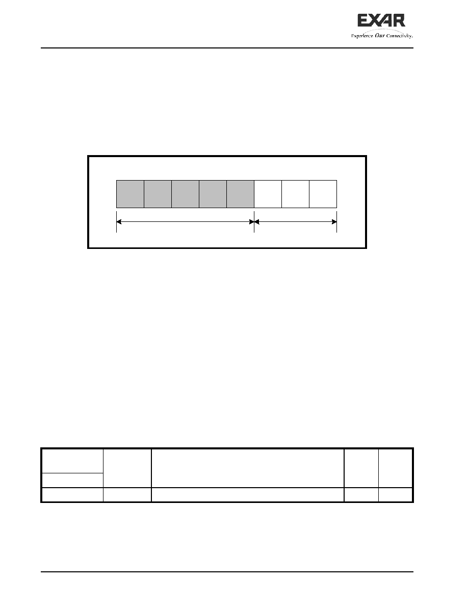
frequency. For best results, register 0x81h can be broken down into two sub-registers with the MSB being bits
D[7:3] and the LSB being bits D[2:0] as shown in Figure 25. Note: Bit D[7] is a reserved bit.
FIGURE 25. REGISTER 0X81H SUB REGISTERS
Programming Examples:
Example 1: Changing bits D[7:3]
If bits D[7:3] are the only values within the register that will change in a WRITE process, the microprocessor
only needs to initiate ONE write operation.
Example 2: Changing bits D[2:0]
If bits D[2:0] are the only values within the register that will change in a WRITE process, the microprocessor
only needs to initiate ONE write operation.
Example 3: Changing bits within the MSB and LSB
In this scenario, one must initiate TWO write operations such that the MSB and LSB do not change within ONE
write cycle. It is recommended that the MSB and LSB be treated as two independent sub-registers. One can
either change the clock selection (MSB) and then change bits D[2:0] (LSB) on the SECOND write, or vice-
versa. No order or sequence is necessary.
TABLE 36: MICROPROCESSOR REGISTER #129, BIT DESCRIPTION
REGISTER ADDRESS
10000001
NAME
FUNCTION
REGISTER
TYPE
RESET
VALUE
BIT #
D7
Reserved
R/W
0
D0
D1
D2
D3
D4
D5
D6
D7
MSB
LSB
Clock Selection Bits
ExLOS, ICT
相关PDF资料 |
PDF描述 |
|---|---|
| XRT83SH314IB-F | IC LIU T1/E1/J1 14CH 304TBGA |
| XRT83SH38IB-F | IC LIU SH T1/E1/J1 8CH 225BGA |
| XRT86L30IV-F | IC LIU/FRAMER TI/E1/J1 SGL 128LQ |
| XRT86VL30IV-F | IC FRAMR/LIU T1/E1/J1 QD 128LQFP |
| XRT86VL32IB-F | IC LIU/FRAMER T1/E1/J1 2CH 225BG |
相关代理商/技术参数 |
参数描述 |
|---|---|
| XRT83L38IV | 制造商:EXAR 制造商全称:EXAR 功能描述:OCTAL T1/E1/J1 LH/SH TRANSCEIVER WITH CLOCK RECOVERY AND JITTER ATTENUATOR |
| XRT83SH314 | 制造商:EXAR 制造商全称:EXAR 功能描述:14-CHANNEL T1/E1/J1 SHORT-HAUL LINE INTERFACE UNIT |
| XRT83SH314_0610 | 制造商:EXAR 制造商全称:EXAR 功能描述:14-CHANNEL T1/E1/J1 SHORT-HAUL LINE INTERFACE UNIT |
| XRT83SH314ES | 功能描述:外围驱动器与原件 - PCI 14 CHT1/E1LIU SH RoHS:否 制造商:PLX Technology 工作电源电压: 最大工作温度: 安装风格:SMD/SMT 封装 / 箱体:FCBGA-1156 封装:Tray |
| XRT83SH314IB | 功能描述:外围驱动器与原件 - PCI RoHS:否 制造商:PLX Technology 工作电源电压: 最大工作温度: 安装风格:SMD/SMT 封装 / 箱体:FCBGA-1156 封装:Tray |
发布紧急采购,3分钟左右您将得到回复。