参数资料
| 型号: | XRT94L31IB-L |
| 厂商: | Exar Corporation |
| 文件页数: | 122/133页 |
| 文件大小: | 0K |
| 描述: | IC MAPPER DS3/E3/STS-1 504TBGA |
| 标准包装: | 24 |
| 应用: | 网络切换 |
| 接口: | 总线 |
| 电源电压: | 3.14 V ~ 3.47 V |
| 封装/外壳: | 504-LBGA |
| 供应商设备封装: | 504-TBGA(35x35) |
| 包装: | 托盘 |
| 安装类型: | 表面贴装 |
第1页第2页第3页第4页第5页第6页第7页第8页第9页第10页第11页第12页第13页第14页第15页第16页第17页第18页第19页第20页第21页第22页第23页第24页第25页第26页第27页第28页第29页第30页第31页第32页第33页第34页第35页第36页第37页第38页第39页第40页第41页第42页第43页第44页第45页第46页第47页第48页第49页第50页第51页第52页第53页第54页第55页第56页第57页第58页第59页第60页第61页第62页第63页第64页第65页第66页第67页第68页第69页第70页第71页第72页第73页第74页第75页第76页第77页第78页第79页第80页第81页第82页第83页第84页第85页第86页第87页第88页第89页第90页第91页第92页第93页第94页第95页第96页第97页第98页第99页第100页第101页第102页第103页第104页第105页第106页第107页第108页第109页第110页第111页第112页第113页第114页第115页第116页第117页第118页第119页第120页第121页当前第122页第123页第124页第125页第126页第127页第128页第129页第130页第131页第132页第133页
XRT94L31
89
REV. 1.0.1
3-CHANNEL DS3/E3/STS-1 TO STS-3/STM-1 MAPPER IC
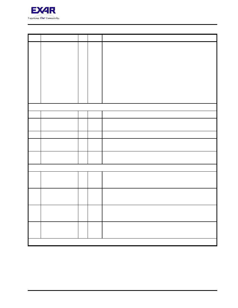
F7
REFCLK45
I
TTL
DS3 Reference Clock Input for the Jitter Attenuator within the DS3/
E3 Mapper Block:
To operate any of the channels of the XRT94L31 in the DS3 Mode, apply
a clock signal with a frequency of 44.736±20ppm to this input pin.
This input pin functions as the timing reference for the DS3/E3/STS-1 Jit-
ter Attenuator (within the DS3/E3 Mapper block) for DS3 applications.
For DS3 Applications, the DS3/E3 Framer block will use this input clock
signal, as a timing source in order to transmit the DS3 AIS Pattern, in the
Egress Direction (e.g., from the XRT94L31 to the DS3/E3/STS-1 LIU
IC).
If the user does not intend to operate any of the three (3) channels in the
DS3 Mode, or if the user intends to configure the XRT94L31 to operate
in the SFM Mode, connect this input pin to GND.
BOUNDARY SCAN
F5
TDO
O
CMOS
Test Data Out: Boundary Scan Test data output
F4
TDI
I
TTL
TEST Data In: Boundary Scan Test data input:
NOTE: This input pin should be pulled "Low" for normal operation.
D3
TRST
I
TTL
JTAG Test Reset Input
E4
TCK
I
TTL
Test clock: Boundary Scan clock inputNote:
NOTE: This input pin should be pulled "Low" for normal operation.
E5
TMS
I
TTL
Test Mode Select: Boundary Scan Mode Select inputNote:
NOTE: This input pin should be pulled "Low" for normal operation.
FILTERING CAPACITORS
U6
RXCAPP
I
ANA-
LOG
External Loop Capacitor for Receive PLL:
This pin connects to the positive side of the external capacitor, which is
used to minimize jitter peaking.
U5
RXCAPN
I
ANA-
LOG
External Loop Capacitor for Receive PLL:
This pin connects to the negative side of the external capacitor, which is
used to minimize jitter peaking.
W6
RXCAPP_R
I
ANAL0
OG
External Redundant Loop Capacitor for Receive PLL:
This pin connects to the positive side of the external capacitor, which is
used to minimize jitter peaking.
W5
RXCAPN_R
I
ANA-
LOG
External Redundant Loop Capacitor for Receive PLL:
This pin connects to the negative side of the external capacitor, which is
used to minimize jitter peaking.
MISCELLANEOUS PINS
PIN DESCRIPTION OF THE XRT94L31 (REV. B)
PIN #
SIGNAL NAME
I/O
TYPE
DESCRIPTION
相关PDF资料 |
PDF描述 |
|---|---|
| XRT94L33IB-L | IC MAPPER DS3/E3/STS-1 504TBGA |
| XRT94L43IB-F | IC MAPPER SONET/SDH OC12 516BGA |
| XS1-G02B-FB144-I4 | IC MCU 32BIT 16KB OTP 144FBGA |
| XTR114U/2K5 | IC 4-20MA I-TRANSMITTER 14-SOIC |
| ZXHF5000JB24TC | IC SWITCH QUAD 2X1 24QFN |
相关代理商/技术参数 |
参数描述 |
|---|---|
| XRT94L33 | 制造商:EXAR 制造商全称:EXAR 功能描述:-CHANNEL DS3/E3/STS-1 TO STS-3/STM-1 MAPPER - SONET REGISTERS |
| XRT94L33_06 | 制造商:EXAR 制造商全称:EXAR 功能描述:3-CHANNEL DS3/E3/STS-1 TO STS-3/STM-1 MAPPER IC DATA SHEET |
| XRT94L33_07 | 制造商:EXAR 制造商全称:EXAR 功能描述:3-CHANNEL DS3/E3/STS-1 TO STS-3/STM-1 MAPPER - ATM REGISTERS |
| XRT94L33_1 | 制造商:EXAR 制造商全称:EXAR 功能描述:3-CHANNEL DS3/E3/STS-1 TO STS-3/STM-1 MAPPER ATM/PPP - HARWARE MANUAL |
| XRT94L33_2 | 制造商:EXAR 制造商全称:EXAR 功能描述:3-CHANNEL DS3/E3/STS-1 TO STS-3/STM-1 MAPPER - SDH REGISTERS |
发布紧急采购,3分钟左右您将得到回复。