- 您现在的位置:买卖IC网 > PDF目录48109 > YSS943-VZ SPECIALTY CONSUMER CIRCUIT, PQFP144 PDF资料下载
参数资料
| 型号: | YSS943-VZ |
| 元件分类: | 消费家电 |
| 英文描述: | SPECIALTY CONSUMER CIRCUIT, PQFP144 |
| 封装: | LEAD FREE, PLASTIC, LQFP-144 |
| 文件页数: | 19/36页 |
| 文件大小: | 831K |
| 代理商: | YSS943-VZ |
第1页第2页第3页第4页第5页第6页第7页第8页第9页第10页第11页第12页第13页第14页第15页第16页第17页第18页当前第19页第20页第21页第22页第23页第24页第25页第26页第27页第28页第29页第30页第31页第32页第33页第34页第35页第36页
YSS944/943/940
26
(5) AC Characteristics
(a)
Power up, Hardware Reset, and clock
No.
Parameter
Symbol
Condition
Min.
Typ.
Max.
Unit
1
nIC time 1
TIC1
Figure 1) below
5
ms
2
nIC time 2
TIC2
Figure 2) below
1
s
3
XI clock frequency
fXIN
12.288
MHz
4
XI clock duty
XDUTY
40
60
%
5
Internal operating
clock cycle
TCLK
Note 1)
1000/178.176
ns
Note 2)
0
1
s
6
Power ON time
TV1V2
Note 3)
1
s
Note 1)
When using recommended XI input and recommended PLL setting. The internal operating clock
frequency is 178.176 MHz.
Note 2)
When Shortcut key barrier diode is not connected
Raise the voltage level 3.3 V power supply(VDD1,AVDDR,AHVDD,AHVDDG)
more than 1.2 V power supply (VDD2,DVDD) even if it is turned ON or OFF.
Note 3)
When Shortcut key barrier diode is connected
Insert a Shortcut key barrier diode with forward voltage of 0.4 V or less between the 3.3 V power
supply (VDD1, AVDDR, AHVDD, and AHVDDG) and 1.2 V power supply (VDD2 and DVDD)
(cathode is VDD1 and anode is VDD2).
Any order and any relation of voltage level is acceptable between 3.3V power supply and 1.2V
power supply when it is turned ON or OFF.
Note 4)
The time interval of power ON or OFF between 3.3V power supply and 1.2V power supply must
be within one second. Only one power keep on supplying, LSI would be damaged.
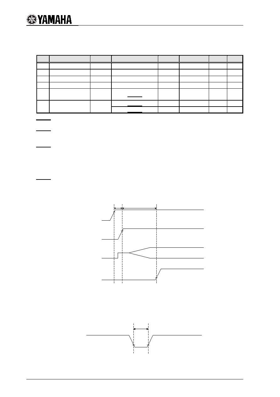
1) At power-on
VDD1, AVDDR,
AHVDD, AHVDDG
XI
nIC
1
VDD2,
DVDD
6
If a crystal oscillator is connected, this includes the time between power supply stabilization and
oscillator stabilization.
Turn on the power when nIC is at low level.
2) In normal operation mode
nIC
2
The XI input and power supply must be stabilized.
If XI oscillation has stopped during initialization in power-down mode, time is required to stabilize
相关PDF资料 |
PDF描述 |
|---|---|
| YSS944-VZ | SPECIALTY CONSUMER CIRCUIT, PQFP144 |
| YSS940-VZ | SPECIALTY CONSUMER CIRCUIT, PQFP144 |
| YSS950-SZ | 0-BIT, 12.5 MHz, OTHER DSP, CQFP64 |
| YSS951-VZ | SPECIALTY CONSUMER CIRCUIT, PQFP48 |
| YTD421B-E | SPECIALTY TELECOM CIRCUIT, PDSO20 |
相关代理商/技术参数 |
参数描述 |
|---|---|
| YSS944 | 制造商:YAMAHA 制造商全称:YAMAHA CORPORATION 功能描述:ADAMB Advanced Digital Audio Multi channel decode processor |
| YSS950 | 制造商:YAMAHA 制造商全称:YAMAHA CORPORATION 功能描述:DAP1 Digital Audio Processor |
| YST 35-22 P24 C3 | 制造商:n/a 功能描述:Thyristor Puck |
| YST025 | 制造商:YEONHO 制造商全称:YEONHO ELECTRONICS 功能描述:2.50mm PITCH CONNECTOR |
| YST025J | 制造商:YEONHO 制造商全称:YEONHO ELECTRONICS 功能描述:2.50mm PITCH CONNECTOR |
发布紧急采购,3分钟左右您将得到回复。