- 您现在的位置:买卖IC网 > PDF目录48110 > YV09T50-0G (POWER-ONE INC) 1-OUTPUT DC-DC REG PWR SUPPLY MODULE PDF资料下载
参数资料
| 型号: | YV09T50-0G |
| 厂商: | POWER-ONE INC |
| 元件分类: | 电源模块 |
| 英文描述: | 1-OUTPUT DC-DC REG PWR SUPPLY MODULE |
| 封装: | ROHS COMPLIANT PACKAGE-15 |
| 文件页数: | 13/13页 |
| 文件大小: | 701K |
| 代理商: | YV09T50-0G |
YV09T50 50A DC-DC POL Converter
5V to 13.8V Input 0.6V to 3.63V Output
Data Sheet
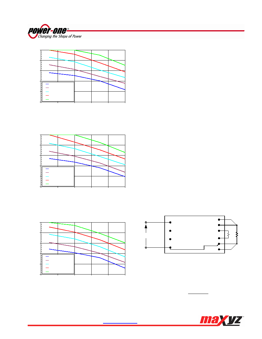
25
30
35
40
45
50
20
30
40
50
60
70
Ambient Temperature, C
Lo
ad
C
u
rr
e
nt
,A
NC
100 LFM (0.5 m/s)
200 LFM (1 m/s)
300 LFM (1.5 m/s)
400 LFM (2 m/s)
Figure 13
Output Current versus Local Ambient
Temperature and Airflow (Vin = 12.0 Vdc,
Vo=1.8Vdc).
25
30
35
40
45
50
20
30
40
50
60
70
Ambient Temperature, C
Lo
ad
C
u
rr
e
nt
,A
NC
100 LFM (0.5 m/s)
200 LFM (1 m/s)
300 LFM (1.5 m/s)
400 LFM (2 m/s)
Figure 14. Output Current versus Local Ambient
Temperature and Airflow (Vin = 12.0 Vdc,
Vo=2.5Vdc).
25
30
35
40
45
50
20
30
40
50
60
70
Ambient Temperature, C
Lo
ad
C
u
rr
e
nt
,A
NC
100 LFM (0.5 m/s)
200 LFM (1 m/s)
300 LFM (1.5 m/s)
400 LFM (2 m/s)
Figure 15. Output Current versus Local Ambient
Temperature and Airflow (Vin = 12.0 Vdc,
Vo=3.3Vdc).
6.
Application Information
6.1
Input and Output Impedance
The POL converter should be connected to the DC
power source via low impedance.
In many
applications, the inductance associated with the
distribution from the power source to the input of the
converter can affect the stability of the converter.
Internally, the converter includes 60F (low ESR
ceramics) of input capacitance which eliminates the
need for external input capacitance. However, if the
distribution of the input voltage to the POL converter
contains high inductance, it is recommended to add
a 150F decoupling capacitor placed as close as
possible to the converter input pins.
A low-ESR
tantalum or POS capacitor connected across the
input pins help ensuring stability of the POL
converter and reduce input ripple voltage.
A 470F POS, tantalum, or ceramic output capacitor
is recommended to improve output ripple and
dynamic response.
It is important to keep low resistance and low
inductance of PCB traces for connecting load to the
output pins of the converter in order to maintain good
load regulation.
6.2
Output Voltage Programming
The output voltage can be programmed from 0.6V to
3.63V by connecting an external resistor RTRIM
between Trim+ pin (Pin 8) and Trim- pin (Pin 7), as
shown in Figure 16.
Figure 16. Programming Output Voltage With A Resistor
The trim resistor RTRIM for a desired output voltage
can be calculated using the following equation:
,
6
.
0
2
.
1
=
OUT
TRIM
V
R
k
Vin
VIN
GND
ON/OFF
VOUT
Power Good
TRIM+
SENSE+
Rload
GND
TRIM-
SENSE-
RTRIM
4,5
12,13
1,2,3
6
9
8
11
4,5
7
10
YV09T50
ZD-02078 Rev 1.0
www.power-one.com
Page 9 of 13
相关PDF资料 |
PDF描述 |
|---|---|
| YV09T50-0 | 1-OUTPUT DC-DC REG PWR SUPPLY MODULE |
| YV09T60-0G | 1-OUTPUT DC-DC REG PWR SUPPLY MODULE |
| YV09T60-0 | 1-OUTPUT DC-DC REG PWR SUPPLY MODULE |
| YV09T60-0EG | 1-OUTPUT DC-DC REG PWR SUPPLY MODULE |
| YV09T60-0E | 1-OUTPUT DC-DC REG PWR SUPPLY MODULE |
相关代理商/技术参数 |
参数描述 |
|---|---|
| YV09T60-0G | 功能描述:DC/DC转换器 0.6-3.63Vout 60A 5V-13.8VIn RoHS:否 制造商:Murata 产品: 输出功率: 输入电压范围:3.6 V to 5.5 V 输入电压(标称): 输出端数量:1 输出电压(通道 1):3.3 V 输出电流(通道 1):600 mA 输出电压(通道 2): 输出电流(通道 2): 安装风格:SMD/SMT 封装 / 箱体尺寸: |
| YV10X5R4A-2 | 制造商:Fujinon 功能描述:5-50mm Day/Night Varifocal Lens |
| YV10X5R4A-2L | 制造商:Fujinon 功能描述:Varifocal Lens |
| YV10X5R4A-SA2L | 制造商:Fujinon 功能描述:5-50mm Day/Night DC Auto Iris Varifocal Lens |
| YV12T25 | 制造商:POWER-ONE 制造商全称:Power-One 功能描述:YV12T25 DC-DC Converter |
发布紧急采购,3分钟左右您将得到回复。