- 您现在的位置:买卖IC网 > PDF目录152475 > 1-100707-01 (SENSITRON SEMICONDUCTOR) DIGITAL TEMP SENSOR-SERIAL, 14BIT(s), SQUARE, SURFACE MOUNT PDF资料下载
参数资料
| 型号: | 1-100707-01 |
| 厂商: | SENSITRON SEMICONDUCTOR |
| 元件分类: | Switch/Digital Output Temperature Sensor |
| 英文描述: | DIGITAL TEMP SENSOR-SERIAL, 14BIT(s), SQUARE, SURFACE MOUNT |
| 封装: | ROHS COMPLIANT PACKAGE, 6 PIN |
| 文件页数: | 7/12页 |
| 文件大小: | 332K |
| 代理商: | 1-100707-01 |
Datasheet SHT21
www.sensirion.com
Version 1.1 – May 2010
4/12
2 Application Information
2.1
Soldering Instructions
The DFN’s die pad (centre pad) and perimeter I/O pads
are fabricated from a planar copper lead-frame by over-
molding leaving the die pad and I/O pads exposed for
mechanical and electrical connection. Both the I/O pads
and die pad should be soldered to the PCB. In order to
prevent oxidation and optimize soldering, the bottom side
of the sensor pads is plated with Ni/Pd/Au.
On the PCB the I/O lands8 should be 0.2mm longer than
the package I/O pads. Inward corners may be rounded to
match the I/O pad shape. The I/O land width should match
the DFN-package I/O-pads width 1:1 and the land for the
die pad should match 1:1 with the DFN package – see
Figure 8.
The solder mask9 design for the land pattern preferably is
of type Non-Solder Mask Defined (NSMD) with solder
mask openings larger than metal pads. For NSMD pads,
the solder mask opening should be about 120m to
150m larger than the pad size, providing a 60m to 75m
design clearance between the copper pad and solder
mask. Rounded portions of package pads should have a
matching rounded solder mask-opening shape to minimize
the risk of solder bridging. For the actual pad dimensions,
each pad on the PCB should have its own solder mask
opening with a web of solder mask between adjacent
pads.
Figure 8 Recommended metal land pattern for SHT2x. Values
in mm. Die pad (centre pad) and NC pads may be left floating or
be connected to ground. The outer dotted line represents the
outer dimension of the DFN package.
For solder paste printing a laser-cut, stainless steel stencil
with electro-polished trapezoidal walls and with 0.125mm
stencil thickness is recommended. For the I/O pads the
stencil apertures should be 0.1mm longer than PCB pads
and positioned with 0.1mm offset away from the centre of
the package. The die pad aperture should cover about 70
– 90% of the pad area – say up to 1.4mm x 2.3mm
8 The land pattern is understood to be the metal layer on the PCB, onto which
the DFN pads are soldered to.
9 The solder mask is understood to be the insulating layer on top of the PCB
covering the connecting lines.
centered on the thermal land area. It can also be split in
two openings.
Due to the low mounted height of the DFN, “no clean”
type 3 solder paste10 is recommended as well as Nitrogen
purge during reflow.
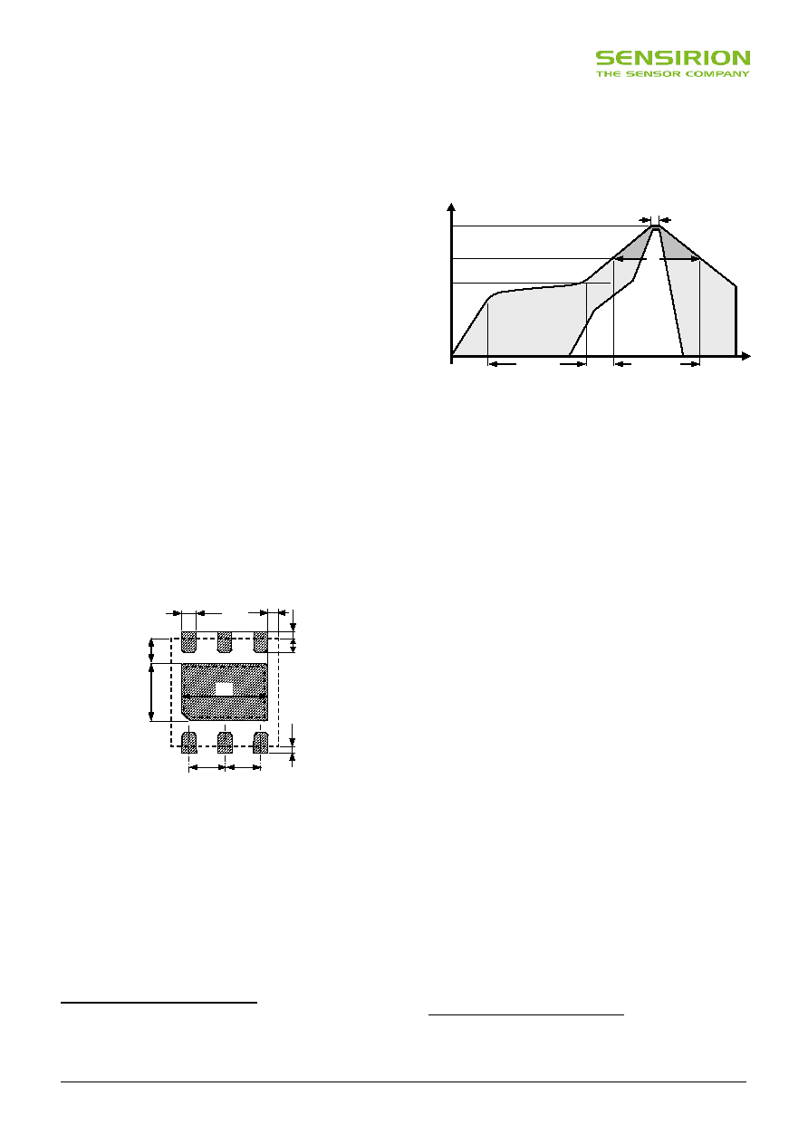
Figure 9 Soldering profile according to JEDEC standard. TP <=
260°C and tP < 40sec for Pb-free assembly. TL < 220°C and tL <
150sec. Ramp-up/down speeds shall be < 5°C/sec.
It is important to note that the diced edge or side faces of
the I/O pads may oxidise over time, therefore a solder fillet
may or may not form. Hence there is no guarantee for
solder joint fillet heights of any kind.
For soldering SHT2x, standard reflow soldering ovens may
be used. The sensor is qualified to withstand soldering
profile according to IPC/JEDEC J-STD-020D with peak
temperatures at 260°C during up to 40sec for Pb-free
assembly in IR/Convection reflow ovens (see Figure 9).
For manual soldering contact time must be limited to 5
seconds at up to 350°C11.
IMPORTANT: After soldering, the devices should be
stored at >75%RH for at least 12h to allow the sensor
element to re-hydrate. Otherwise the sensor may read an
offset that slowly disappears if exposed to ambient
conditions. Alternatively the re-hydration process may be
performed at ambient conditions (>40%RH) during more
than 5 days.
In no case, neither after manual nor reflow soldering, a
board wash shall be applied. Therefore, and as mentioned
above, it is strongly recommended to use “no-clean” solder
paste. In case of applications with exposure of the sensor
to corrosive gases or condensed water (i.e. environments
with high relative humidity) the soldering pads shall be
sealed (e.g. conformal coating) to prevent loose contacts
or short cuts.
10 Solder types are related to the solder particle size in the paste: Type 3 covers
the size range of 25 – 45 m (powder type 42).
11 260°C = 500°F, 350°C = 662°F
1.0
0.3
0.
4
1.
5
0.4
0.
7
0.
2
0.
2
2.4
Te
m
pe
ra
tur
e
Time
tP
TP
TL
TS (max)
tL
preheating
critical zone
相关PDF资料 |
PDF描述 |
|---|---|
| 1-100645-01 | DIGITAL TEMP SENSOR-SERIAL, 14BIT(s), SQUARE, SURFACE MOUNT |
| 1-102154-0 | 50 CONTACT(S), MALE, STRAIGHT TWO PART BOARD CONNECTOR, SOLDER |
| 1-102154-1 | 60 CONTACT(S), MALE, STRAIGHT TWO PART BOARD CONNECTOR, SOLDER |
| 1-102154-2 | 64 CONTACT(S), MALE, STRAIGHT TWO PART BOARD CONNECTOR, SOLDER |
| 1-102321-0 | 50 CONTACT(S), MALE, STRAIGHT TWO PART BOARD CONNECTOR, SOLDER |
相关代理商/技术参数 |
参数描述 |
|---|---|
| 11-007082-000 | 制造商:Amphenol Corporation 功能描述:11-007082-000 - Bulk |
| 11-007-172 | 功能描述:电缆组件 FLAT PIN STAKED FLEX MALE/FEMALE TIN ENDS RoHS:否 制造商:Molex 产品:Power Assemblies 类型:Cable Assembly 连接器端口 A:No Connector 连接器端口 A 管脚计数:4 连接器端口 B:No Connector 连接器端口 B 管脚计数: 型式:Male 线规 - 美国线规(AWG):20, 28 长度:0.305 m 颜色:Black, Red |
| 11-007295-000 | 制造商:Amphenol Corporation 功能描述:11-007295-000 - Bulk |
| 11-007345-000 | 制造商:Amphenol Corporation 功能描述:11-007345-000 - Bulk |
| 11-007368-000 | 制造商:Amphenol Corporation 功能描述:TOOL - Bulk |
发布紧急采购,3分钟左右您将得到回复。