- 您现在的位置:买卖IC网 > PDF目录366173 > 1N6379RL4 (ON SEMICONDUCTOR) 1500 Watt Peak Power Mosorb TM Zener Transient Voltage Suppressors PDF资料下载
参数资料
| 型号: | 1N6379RL4 |
| 厂商: | ON SEMICONDUCTOR |
| 元件分类: | 参考电压二极管 |
| 英文描述: | 1500 Watt Peak Power Mosorb TM Zener Transient Voltage Suppressors |
| 中文描述: | 1500 W, UNIDIRECTIONAL, SILICON, TVS DIODE |
| 封装: | PLASTIC, MOSORB, CASE 41A-04, 2 PIN |
| 文件页数: | 6/8页 |
| 文件大小: | 85K |
| 代理商: | 1N6379RL4 |
1N6373 1N6381 Series (ICTE5 ICTE36, MPTE5 MPTE45)
http://onsemi.com
6
APPLICATION NOTES
RESPONSE TIME
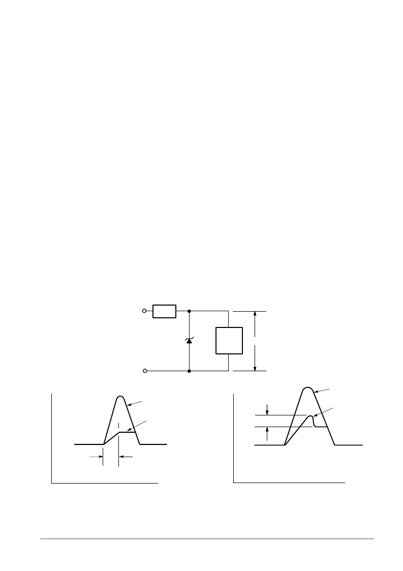
In most applications, the transient suppressor device is
placed in parallel with the equipment or component to be
protected. In this situation, there is a time delay associated
with the capacitance of the device and an overshoot
condition associated with the inductance of the device and
the inductance of the connection method. The capacitance
effect is of minor importance in the parallel protection
scheme because it only produces a time delay in the
transition from the operating voltage to the clamp voltage as
shown in Figure 8.
The inductive effects in the device are due to actual
turn-on time (time required for the device to go from zero
current to full current) and lead inductance. This inductive
effect produces an overshoot in the voltage across the
equipment or component being protected as shown in
Figure 9. Minimizing this overshoot is very important in the
application, since the main purpose for adding a transient
suppressor is to clamp voltage spikes. These devices have
excellent response time, typically in the picosecond range
and negligible inductance. However, external inductive
effects could produce unacceptable overshoot. Proper
circuit layout, minimum lead lengths and placing the
suppressor device as close as possible to the equipment or
components to be protected will minimize this overshoot.
Some input impedance represented by Z
in
is essential to
prevent overstress of the protection device. This impedance
should be as high as possible, without restricting the circuit
operation.
DUTY CYCLE DERATING
The data of Figure 1 applies for non-repetitive conditions
and at a lead temperature of 25
°
C. If the duty cycle increases,
the peak power must be reduced as indicated by the curves
of Figure 7. Average power must be derated as the lead or
ambient temperature rises above 25
°
C. The average power
derating curve normally given on data sheets may be
normalized and used for this purpose.
At first glance the derating curves of Figure 7 appear to be
in error as the 10 ms pulse has a higher derating factor than
the 10 s pulse. However, when the derating factor for a
given pulse of Figure 7 is multiplied by the peak power value
of Figure 1 for the same pulse, the results follow the
expected trend.
TYPICAL PROTECTION CIRCUIT
V
in
V
L
V
V
in
V
in
(TRANSIENT)
V
L
t
d
V
V
L
V
in
(TRANSIENT)
Z
in
LOAD
OVERSHOOT DUE TO
INDUCTIVE EFFECTS
t
D
= TIME DELAY DUE TO CAPACITIVE EFFECT
t
t
Figure 8.
Figure 9.
相关PDF资料 |
PDF描述 |
|---|---|
| 1N6379RL4G | 1500 Watt Peak Power Mosorb TM Zener Transient Voltage Suppressors |
| 1N6380G | 1500 Watt Peak Power Mosorb TM Zener Transient Voltage Suppressors |
| 1N6380RL4 | 1500 Watt Peak Power Mosorb TM Zener Transient Voltage Suppressors |
| 1N6380RL4G | 1500 Watt Peak Power Mosorb TM Zener Transient Voltage Suppressors |
| 1N6381G | 1500 Watt Peak Power Mosorb TM Zener Transient Voltage Suppressors |
相关代理商/技术参数 |
参数描述 |
|---|---|
| 1N6379RL4G | 功能描述:TVS 二极管 - 瞬态电压抑制器 25.9V 1500W Unidirectional RoHS:否 制造商:Vishay Semiconductors 极性:Bidirectional 工作电压: 击穿电压:58.9 V 钳位电压:77.4 V 峰值浪涌电流:38.8 A 系列: 封装 / 箱体:DO-214AB 最小工作温度:- 55 C 最大工作温度:+ 150 C |
| 1N6380 | 功能描述:TVS 二极管 - 瞬态电压抑制器 42.2V 1500W RoHS:否 制造商:Vishay Semiconductors 极性:Bidirectional 工作电压: 击穿电压:58.9 V 钳位电压:77.4 V 峰值浪涌电流:38.8 A 系列: 封装 / 箱体:DO-214AB 最小工作温度:- 55 C 最大工作温度:+ 150 C |
| 1N6380G | 功能描述:TVS 二极管 - 瞬态电压抑制器 42.2V 1500W Unidirectional RoHS:否 制造商:Vishay Semiconductors 极性:Bidirectional 工作电压: 击穿电压:58.9 V 钳位电压:77.4 V 峰值浪涌电流:38.8 A 系列: 封装 / 箱体:DO-214AB 最小工作温度:- 55 C 最大工作温度:+ 150 C |
| 1N6380G | 制造商:ON Semiconductor 功能描述:TVS Diode |
| 1N6380RL4 | 功能描述:TVS 二极管 - 瞬态电压抑制器 42.2V 1500W RoHS:否 制造商:Vishay Semiconductors 极性:Bidirectional 工作电压: 击穿电压:58.9 V 钳位电压:77.4 V 峰值浪涌电流:38.8 A 系列: 封装 / 箱体:DO-214AB 最小工作温度:- 55 C 最大工作温度:+ 150 C |
发布紧急采购,3分钟左右您将得到回复。