- 您现在的位置:买卖IC网 > PDF目录4227 > 24FC1026T-I/SM (Microchip Technology)IC EEPROM 1024KB 1MHZ 8-SOIJ PDF资料下载
参数资料
| 型号: | 24FC1026T-I/SM |
| 厂商: | Microchip Technology |
| 文件页数: | 8/28页 |
| 文件大小: | 0K |
| 描述: | IC EEPROM 1024KB 1MHZ 8-SOIJ |
| 标准包装: | 2,100 |
| 格式 - 存储器: | EEPROMs - 串行 |
| 存储器类型: | EEPROM |
| 存储容量: | 1M (128K x 8) |
| 速度: | 400kHz,1MHz |
| 接口: | I²C,2 线串口 |
| 电源电压: | 1.8 V ~ 5.5 V |
| 工作温度: | -40°C ~ 85°C |
| 封装/外壳: | 8-SOIC(0.209",5.30mm 宽) |
| 供应商设备封装: | 8-SOIJ |
| 包装: | 带卷 (TR) |
第1页第2页第3页第4页第5页第6页第7页当前第8页第9页第10页第11页第12页第13页第14页第15页第16页第17页第18页第19页第20页第21页第22页第23页第24页第25页第26页第27页第28页
�� �
�
�24AA1026/24LC1026/24FC1026�
�5.0� DEVICE� ADDRESSING�
�A� control� byte� is� the� first� byte� received� following� the�
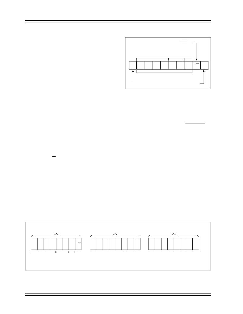
�FIGURE� 5-1:�
�CONTROL� BYTE�
�FORMAT�
�Start� condition� from� the� master� device� (� Figure� 5-1� ).�
�The� control� byte� consists� of� a� 4-bit� control� code;� for� the�
�24XX1026,� this� is� set� as� ‘� 1010� ’� binary� for� read� and�
�write� operations.� The� next� two� bits� of� the� control� byte�
�are� the� Chip� Select� bits� (A2,� A1).� The� Chip� Select� bits�
�Control� Code�
�Read/Write� Bit�
�Chip� Block�
�Select� Select�
�Bits� Bit�
�allow� the� use� of� up� to� four� 24XX1026� devices� on� the�
�same� bus� and� are� used� to� select� which� device� is�
�S�
�1�
�0�
�1�
�0�
�A2�
�A1�
�B0� R/W� ACK�
�accessed.� The� Chip� Select� bits� in� the� control� byte� must�
�correspond� to� the� logic� levels� on� the� corresponding� A2�
�Slave� Address�
�and� A1� pins� for� the� device� to� respond.� These� bits� are� in�
�effect� the� two� Most� Significant� bits� (MSb)� of� the� word�
�address.� The� next� bit� of� the� control� byte� is� the� block�
�Start� Bit�
�Acknowledge� Bit�
�select� bit� (B0).� This� bit� acts� as� the� A16� address� bit� for�
�accessing� the� entire� array.�
�The� last� bit� of� the� control� byte� defines� the� operation� to�
�be� performed.� When� set� to� a� one,� a� read� operation� is�
�selected,� and� when� set� to� a� zero,� a� write� operation� is�
�selected.� The� next� two� bytes� received� define� the�
�address� of� the� first� data� byte� (� Figure� 5-2� ).� The� upper�
�address� bits� are� transferred� first,� followed� by� the� Least�
�Significant� bits� (LSb).�
�Following� the� Start� condition,� the� 24XX1026� monitors�
�the� SDA� bus� checking� the� device� type� identifier� being�
�transmitted.� Upon� receiving� a� ‘� 1010� ’� code� and�
�appropriate� device� select� bits,� the� slave� device� outputs�
�an� Acknowledge� signal� on� the� SDA� line.� Depending� on�
�the� state� of� the� R/W� bit,� the� 24XX1026� will� select� a� read�
�or� write� operation.�
�This� device� has� an� internal� addressing� boundary�
�limitation� that� is� divided� into� two� segments� of� 512K� bits.�
�Block� select� bit� ‘B0’� is� used� to� control� access� to� each�
�segment.�
�5.1� Contiguous� Addressing� Across�
�Multiple� Devices�
�The� Chip� Select� bits� A2� and� A1� can� be� used� to� expand�
�the� contiguous� address� space� for� up� to� 4� Mbit� by� add-�
�ing� up� to� four� 24XX1026’s� on� the� same� bus.� In� this�
�case,� software� can� use� A1� of� the� control byte� as�
�address� bit� A17� and� A2� as� address� bit� A18.� It� is� not�
�possible� to� sequentially� read� across� device� boundar-�
�ies.�
�Each� device� has� internal� addressing� boundary�
�limitations.� This� divides� each� part� into� two� segments� of�
�512K� bits.� The� block� select� bit� ‘B0’� controls� access� to�
�each� “half”.�
�Sequential� read� operations� are� limited� to� 512K� blocks.�
�To� read� through� four� devices� on� the� same� bus,� eight�
�random� Read� commands� must� be� given.�
�FIGURE� 5-2:�
�ADDRESS� SEQUENCE� BIT� ASSIGNMENTS�
�Control� Byte�
�Address� High� Byte�
�Address� Low� Byte�
�0� R/W�
�1�
�0�
�1�
�0�
�A�
�2�
�A�
�1�
�B�
�A� A� A� A� A� A�
�15� 14� 13� 12� 11� 10�
�A�
�9�
�A�
�8�
�A�
�7�
�?�
�?�
�?�
�?�
�?�
�?�
�A�
�0�
�Control�
�Code�
�DS22270C-page� 8�
�Chip� Block�
�Select� Select�
�Bits� Bit�
�?� 2011-2012� Microchip� Technology� Inc.�
�相关PDF资料 |
PDF描述 |
|---|---|
| AMC10DTEN | CONN EDGECARD 20POS .100 EYELET |
| SST25VF064C-80-4C-Q2AE-T | IC FLASH SER 64M DUAL I/O 8WSON |
| AMC10DTEH | CONN EDGECARD 20POS .100 EYELET |
| SST25VF064C-80-4C-Q2AE | IC FLASH SER 64M DUAL I/O 8WSON |
| ASC60DRTS | CONN EDGECARD 120PS .100 DIP SLD |
相关代理商/技术参数 |
参数描述 |
|---|---|
| 24FC128 | 制造商:MICROCHIP 制造商全称:Microchip Technology 功能描述:128K I2C CMOS Serial EEPROM |
| 24FC128-E/CS15K | 制造商:MICROCHIP 制造商全称:Microchip Technology 功能描述:128K I2Ca?¢ CMOS Serial EEPROM |
| 24FC128-E/MC | 制造商:MICROCHIP 制造商全称:Microchip Technology 功能描述:128K I2C CMOS Serial EEPROM |
| 24FC128E/MF | 制造商:未知厂家 制造商全称:未知厂家 功能描述:EEPROM |
| 24FC128-E/MF | 制造商:MICROCHIP 制造商全称:Microchip Technology 功能描述:128K I2C CMOS Serial EEPROM |
发布紧急采购,3分钟左右您将得到回复。