- 您现在的位置:买卖IC网 > PDF目录298280 > 24LCS21P I2C Serial EEPROM PDF资料下载
参数资料
| 型号: | 24LCS21P |
| 英文描述: | I2C Serial EEPROM |
| 中文描述: | I2C串行EEPROM的 |
| 文件页数: | 10/12页 |
| 文件大小: | 159K |
| 代理商: | 24LCS21P |
1999 Microchip Technology Inc.
DS21127D-page 7
24LCS21
3.1.6
SLAVE ADDRESS
After generating a START condition, the bus master
transmits the slave address consisting of a 7-bit device
code (1010000) for the 24LCS21.
The eighth bit of slave address determines whether the
master device wants to read or write to the 24LCS21
The 24LCS21 monitors the bus for its corresponding
slave
address
continuously.
It
generates
an
acknowledge bit if the slave address was true and it is
not in a programming mode.
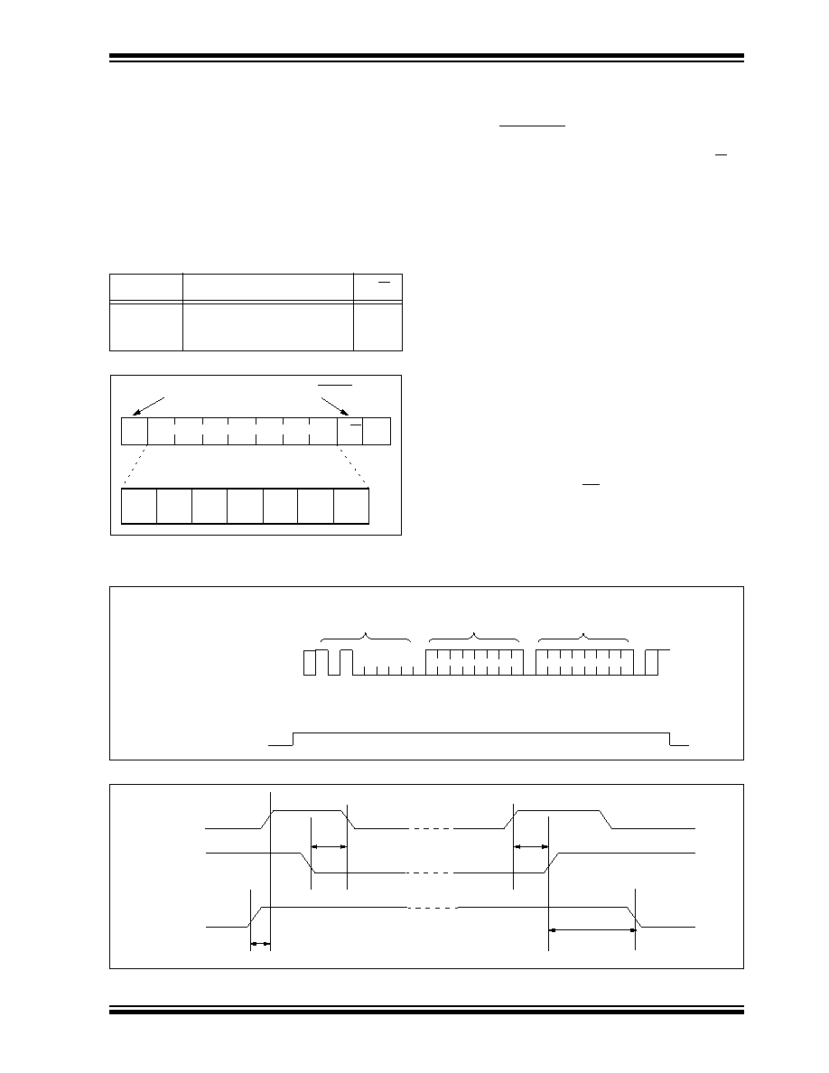
FIGURE 3-5: CONTROL BYTE ALLOCATION
4.0
WRITE OPERATION
4.1
Byte Write
Following the start signal from the master, the slave
address (4 bits), three zero bits (000) and the R/W bit
which is a logic low are placed onto the bus by the
master transmitter. This indicates to the addressed
slave receiver that a byte with a word address will follow
after it has generated an acknowledge bit during the
ninth clock cycle. Therefore, the next byte transmitted
by the master is the word address and will be written
into the address pointer of the 24LCS21. After receiv-
ing another acknowledge signal from the 24LCS21 the
master device will transmit the data word to be written
into the addressed memory location. The 24LCS21
acknowledges again and the master generates a stop
condition. This initiates the internal write cycle, and dur-
ing this time the 24LCS21 will not generate acknowl-
edge signals (Figure 4-1).
It is required that VCLK be held at a logic high level
during command and data transfer in order to program
the device. This applies to both byte write and page
write operation. Note, however, that the VCLK is
ignored during the self-timed program operation.
Changing VCLK from high to low during the self-timed
program operation will not halt programming of the
device.
Operation
Slave Address
R/W
Read
1010000
1
Write
1010000
0
SLAVE ADDRESS
101
00
0
R/W
A
START
READ/WRITE
FIGURE 4-1: BYTE WRITE
FIGURE 4-2: VCLK WRITE ENABLE TIMING
BUS ACTIVITY:
MASTER
SDA LINE
BUS ACTIVITY:
CONTROL
BYTE
WORD
ADDRESS
DATA
S
T
O
P
S
T
A
R
T
A
C
K
S
P
A
C
K
A
C
K
VCLK
TSPVL
TSU:STO
THD:STA
TVHST
VCLK
SDA
IN
SCL
This Material Copyrighted by Its Respective Manufacturer
相关PDF资料 |
PDF描述 |
|---|---|
| 24LCS21SN | I2C Serial EEPROM |
| 24LCS21TISN | I2C Serial EEPROM |
| 24LCS21TSN | I2C Serial EEPROM |
| 24LCS22A | 24LCS22A Datasheet |
| 24PCAFA1D | Industrial Control IC |
相关代理商/技术参数 |
参数描述 |
|---|---|
| 24LCS22A-I/P | 功能描述:电可擦除可编程只读存储器 VESA E-EDID RoHS:否 制造商:Atmel 存储容量:2 Kbit 组织:256 B x 8 数据保留:100 yr 最大时钟频率:1000 KHz 最大工作电流:6 uA 工作电源电压:1.7 V to 5.5 V 最大工作温度:+ 85 C 安装风格:SMD/SMT 封装 / 箱体:SOIC-8 |
| 24LCS22A-I/PG | 功能描述:电可擦除可编程只读存储器 VESA E-EDID Lead Free Package RoHS:否 制造商:Atmel 存储容量:2 Kbit 组织:256 B x 8 数据保留:100 yr 最大时钟频率:1000 KHz 最大工作电流:6 uA 工作电源电压:1.7 V to 5.5 V 最大工作温度:+ 85 C 安装风格:SMD/SMT 封装 / 箱体:SOIC-8 |
| 24LCS22A-I/SN | 功能描述:电可擦除可编程只读存储器 VESA E-EDID RoHS:否 制造商:Atmel 存储容量:2 Kbit 组织:256 B x 8 数据保留:100 yr 最大时钟频率:1000 KHz 最大工作电流:6 uA 工作电源电压:1.7 V to 5.5 V 最大工作温度:+ 85 C 安装风格:SMD/SMT 封装 / 箱体:SOIC-8 |
| 24LCS22A-I/SNG | 功能描述:电可擦除可编程只读存储器 VESA E-EDID Lead Free Package RoHS:否 制造商:Atmel 存储容量:2 Kbit 组织:256 B x 8 数据保留:100 yr 最大时钟频率:1000 KHz 最大工作电流:6 uA 工作电源电压:1.7 V to 5.5 V 最大工作温度:+ 85 C 安装风格:SMD/SMT 封装 / 箱体:SOIC-8 |
| 24LCS22AT-I/SN | 功能描述:电可擦除可编程只读存储器 VESA E-EDID RoHS:否 制造商:Atmel 存储容量:2 Kbit 组织:256 B x 8 数据保留:100 yr 最大时钟频率:1000 KHz 最大工作电流:6 uA 工作电源电压:1.7 V to 5.5 V 最大工作温度:+ 85 C 安装风格:SMD/SMT 封装 / 箱体:SOIC-8 |
发布紧急采购,3分钟左右您将得到回复。