- 您现在的位置:买卖IC网 > PDF目录298280 > 24LCS21P I2C Serial EEPROM PDF资料下载
参数资料
| 型号: | 24LCS21P |
| 英文描述: | I2C Serial EEPROM |
| 中文描述: | I2C串行EEPROM的 |
| 文件页数: | 2/12页 |
| 文件大小: | 159K |
| 代理商: | 24LCS21P |
24LCS21
DS21127D-page 10
1999 Microchip Technology Inc.
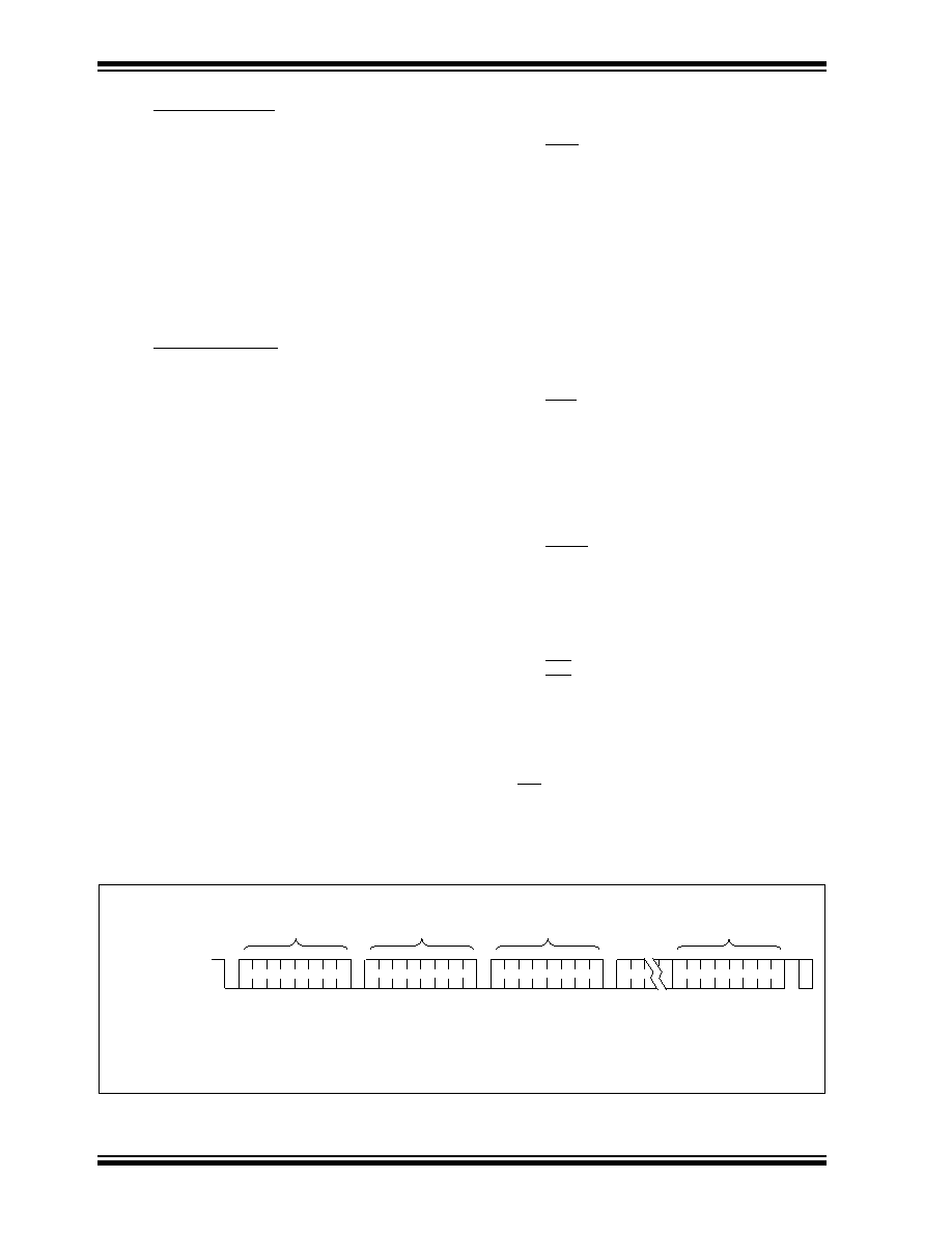
7.3
Sequential Read
Sequential reads are initiated in the same way as a
random read except that after the 24LCS21 transmits
the rst data byte, the master issues an acknowledge
as opposed to a stop condition in a random read. This
directs the 24LCS21 to transmit the next sequentially
addressed 8-bit word (Figure 8-1).
To provide sequential reads the 24LCS21 contains an
internal address pointer which is incremented by one at
the completion of each operation. This address pointer
allows the entire memory contents to be serially read
during one operation.
7.4
Noise Protection
The 24LCS21 employs a VCC threshold detector circuit
which disables the internal erase/write logic if the VCC
is below 1.5 volts at nominal conditions.
The SDA, SCL and VCLK inputs have Schmitt trigger
and lter circuits which suppress noise spikes to assure
proper device operation even on a noisy bus.
8.0
PIN DESCRIPTIONS
8.1
SDA
This pin is used to transfer addresses and data into and
out of the device, when the device is in the bi-direc-
tional Mode. In the Transmit-Only Mode, which only
allows data to be read from the device, data is also
transferred on the SDA pin. This pin is an open drain
terminal, therefore the SDA bus requires a pullup
resistor to VCC (typical 10 K
for 100 kHz, 2 K for
400 kHz).
For normal data transfer in the bi-directional Mode,
SDA is allowed to change only during SCL low.
Changes during SCL high are reserved for indicating
the START and STOP conditions.
8.2
SCL
This pin is the clock input for the bi-directional Mode,
and is used to synchronize data transfer to and from the
device. It is also used as the signaling input to switch
the device from the Transmit Only Mode to the bi-direc-
tional Mode. It must remain high for the chip to continue
operation in the Transmit Only Mode.
8.3
VCLK
This pin is the clock input for the Transmit Only Mode
(DDC1). In the Transmit Only Mode, each bit is clocked
out on the rising edge of this signal. In the bi-directional
Mode, a high logic level is required on this pin to enable
write capability.
8.4
WP
This pin is used for exible write protection of the
24LCS21. When the last memory location (7Fh) is
written with any data, this pin is enabled and
determines the write capability of the 24LCS21
The WP pin has an internal pull up resistor which will
allow write capability (assuming VCLK = 1) at all times
if this pin is oated.
FIGURE 8-1: SEQUENTIAL READ
A
C
K
P
BUS ACTIVITY
MASTER
SDA LINE
BUS ACTIVITY
CONTROL
BYTE
DATA n
DATA n+1
DATA n+2
DATA n+X
A
C
K
A
C
K
A
C
K
N
O
A
C
K
S
T
O
P
This Material Copyrighted by Its Respective Manufacturer
相关PDF资料 |
PDF描述 |
|---|---|
| 24LCS21SN | I2C Serial EEPROM |
| 24LCS21TISN | I2C Serial EEPROM |
| 24LCS21TSN | I2C Serial EEPROM |
| 24LCS22A | 24LCS22A Datasheet |
| 24PCAFA1D | Industrial Control IC |
相关代理商/技术参数 |
参数描述 |
|---|---|
| 24LCS22A-I/P | 功能描述:电可擦除可编程只读存储器 VESA E-EDID RoHS:否 制造商:Atmel 存储容量:2 Kbit 组织:256 B x 8 数据保留:100 yr 最大时钟频率:1000 KHz 最大工作电流:6 uA 工作电源电压:1.7 V to 5.5 V 最大工作温度:+ 85 C 安装风格:SMD/SMT 封装 / 箱体:SOIC-8 |
| 24LCS22A-I/PG | 功能描述:电可擦除可编程只读存储器 VESA E-EDID Lead Free Package RoHS:否 制造商:Atmel 存储容量:2 Kbit 组织:256 B x 8 数据保留:100 yr 最大时钟频率:1000 KHz 最大工作电流:6 uA 工作电源电压:1.7 V to 5.5 V 最大工作温度:+ 85 C 安装风格:SMD/SMT 封装 / 箱体:SOIC-8 |
| 24LCS22A-I/SN | 功能描述:电可擦除可编程只读存储器 VESA E-EDID RoHS:否 制造商:Atmel 存储容量:2 Kbit 组织:256 B x 8 数据保留:100 yr 最大时钟频率:1000 KHz 最大工作电流:6 uA 工作电源电压:1.7 V to 5.5 V 最大工作温度:+ 85 C 安装风格:SMD/SMT 封装 / 箱体:SOIC-8 |
| 24LCS22A-I/SNG | 功能描述:电可擦除可编程只读存储器 VESA E-EDID Lead Free Package RoHS:否 制造商:Atmel 存储容量:2 Kbit 组织:256 B x 8 数据保留:100 yr 最大时钟频率:1000 KHz 最大工作电流:6 uA 工作电源电压:1.7 V to 5.5 V 最大工作温度:+ 85 C 安装风格:SMD/SMT 封装 / 箱体:SOIC-8 |
| 24LCS22AT-I/SN | 功能描述:电可擦除可编程只读存储器 VESA E-EDID RoHS:否 制造商:Atmel 存储容量:2 Kbit 组织:256 B x 8 数据保留:100 yr 最大时钟频率:1000 KHz 最大工作电流:6 uA 工作电源电压:1.7 V to 5.5 V 最大工作温度:+ 85 C 安装风格:SMD/SMT 封装 / 箱体:SOIC-8 |
发布紧急采购,3分钟左右您将得到回复。