- 您现在的位置:买卖IC网 > PDF目录298280 > 24LCS21P I2C Serial EEPROM PDF资料下载
参数资料
| 型号: | 24LCS21P |
| 英文描述: | I2C Serial EEPROM |
| 中文描述: | I2C串行EEPROM的 |
| 文件页数: | 7/12页 |
| 文件大小: | 159K |
| 代理商: | 24LCS21P |
24LCS21
DS21127D-page 4
1999 Microchip Technology Inc.
2.0
FUNCTIONAL DESCRIPTION
The
24LCS21
operates
in
two
modes,
the
Transmit-Only Mode and the bi-directional Mode. There
is a separate two wire protocol to support each mode,
each having a separate clock input but sharing a com-
mon data line (SDA). The device enters the Trans-
mit-Only Mode upon power-up. In this mode, the device
transmits data bits on the SDA pin in response to a
clock signal on the VCLK pin. The device will remain in
this mode until a valid high to low transition is placed on
the SCL input. When a valid transition on SCL is recog-
nized, the device will switch into the bi-directional
Mode. The only way to switch the device back to the
Transmit-Only Mode is to remove power from the
device.
2.1
Transmit-Only Mode
The device will power up in the Transmit-Only Mode at
address 00H. This mode supports a unidirectional two
wire protocol for continuous transmission of the
contents of the memory array. This device requires that
it be initialized prior to valid data being sent in the
Transmit-Only Mode (see Initialization Procedure,
below). In this mode, data is transmitted on the SDA
pin in 8-bit bytes, with each byte followed by a ninth, null
bit (Figure 2-1). The clock source for the Transmit-Only
Mode is provided on the VCLK pin, and a data bit is out-
put on the rising edge on this pin. The eight bits in each
byte are transmitted most signicant bit rst. Each byte
within the memory array will be output in sequence.
When the last byte in the memory array is transmitted,
the internal address pointers will wrap around to the
rst memory location (00H) and continue. The bi-direc-
tional Mode Clock (SCL) pin must be held high for the
device to remain in the Transmit-Only Mode.
2.2
Initialization Procedure
After VCC has stabilized, the device will be in the
Transmit-Only Mode. Nine clock cycles on the VCLK
pin must be given to the device for it to perform internal
sychronization. During this period, the SDA pin will be
in a high impedance state. On the rising edge of the
tenth clock cycle, the device will output the rst valid
data bit which will be the most signicant bit in address
00h. (Figure 2-2).
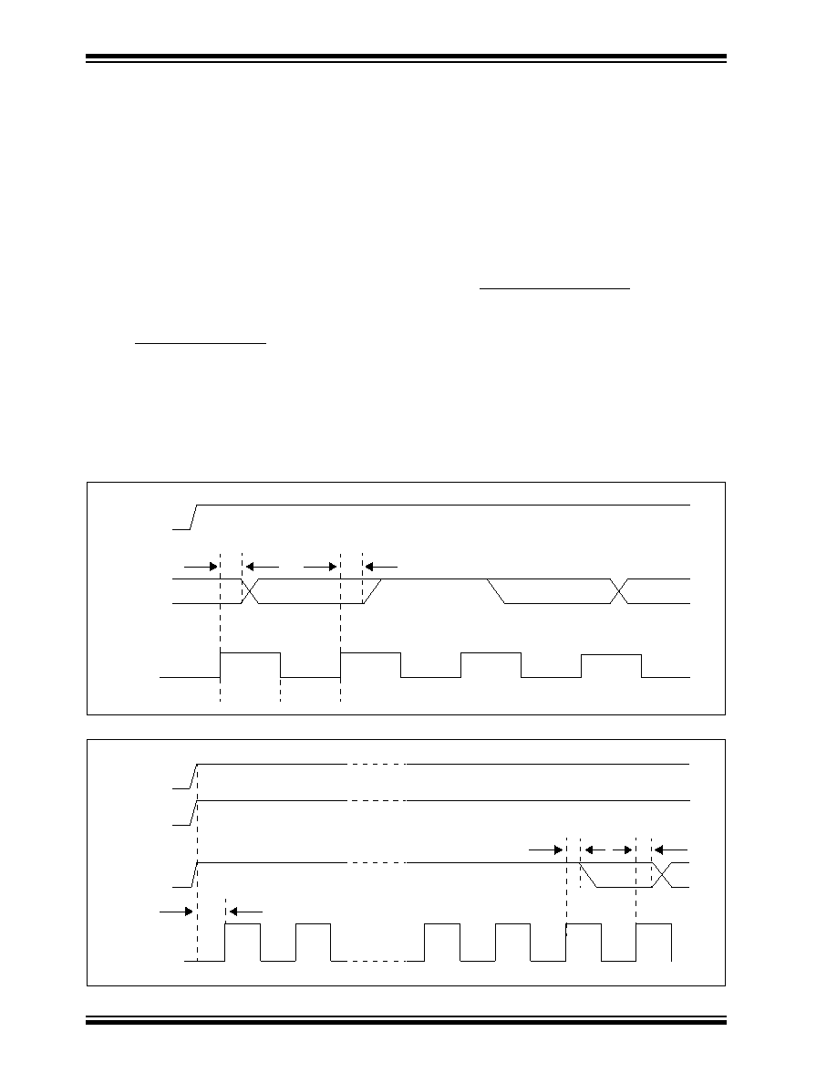
FIGURE 2-1: TRANSMIT ONLY MODE
FIGURE 2-2: DEVICE INITIALIZATION
SCL
SDA
VCLK
TVAA
Bit 1 (LSB)
Null Bit
Bit 1 (MSB)
Bit 7
TVLOW
TVHIGH
TVAA
Bit 8
Bit 7
High Impedance for 9 clock cycles
TVPU
12
89
10
11
SCL
SDA
VCLK
Vcc
This Material Copyrighted by Its Respective Manufacturer
相关PDF资料 |
PDF描述 |
|---|---|
| 24LCS21SN | I2C Serial EEPROM |
| 24LCS21TISN | I2C Serial EEPROM |
| 24LCS21TSN | I2C Serial EEPROM |
| 24LCS22A | 24LCS22A Datasheet |
| 24PCAFA1D | Industrial Control IC |
相关代理商/技术参数 |
参数描述 |
|---|---|
| 24LCS22A-I/P | 功能描述:电可擦除可编程只读存储器 VESA E-EDID RoHS:否 制造商:Atmel 存储容量:2 Kbit 组织:256 B x 8 数据保留:100 yr 最大时钟频率:1000 KHz 最大工作电流:6 uA 工作电源电压:1.7 V to 5.5 V 最大工作温度:+ 85 C 安装风格:SMD/SMT 封装 / 箱体:SOIC-8 |
| 24LCS22A-I/PG | 功能描述:电可擦除可编程只读存储器 VESA E-EDID Lead Free Package RoHS:否 制造商:Atmel 存储容量:2 Kbit 组织:256 B x 8 数据保留:100 yr 最大时钟频率:1000 KHz 最大工作电流:6 uA 工作电源电压:1.7 V to 5.5 V 最大工作温度:+ 85 C 安装风格:SMD/SMT 封装 / 箱体:SOIC-8 |
| 24LCS22A-I/SN | 功能描述:电可擦除可编程只读存储器 VESA E-EDID RoHS:否 制造商:Atmel 存储容量:2 Kbit 组织:256 B x 8 数据保留:100 yr 最大时钟频率:1000 KHz 最大工作电流:6 uA 工作电源电压:1.7 V to 5.5 V 最大工作温度:+ 85 C 安装风格:SMD/SMT 封装 / 箱体:SOIC-8 |
| 24LCS22A-I/SNG | 功能描述:电可擦除可编程只读存储器 VESA E-EDID Lead Free Package RoHS:否 制造商:Atmel 存储容量:2 Kbit 组织:256 B x 8 数据保留:100 yr 最大时钟频率:1000 KHz 最大工作电流:6 uA 工作电源电压:1.7 V to 5.5 V 最大工作温度:+ 85 C 安装风格:SMD/SMT 封装 / 箱体:SOIC-8 |
| 24LCS22AT-I/SN | 功能描述:电可擦除可编程只读存储器 VESA E-EDID RoHS:否 制造商:Atmel 存储容量:2 Kbit 组织:256 B x 8 数据保留:100 yr 最大时钟频率:1000 KHz 最大工作电流:6 uA 工作电源电压:1.7 V to 5.5 V 最大工作温度:+ 85 C 安装风格:SMD/SMT 封装 / 箱体:SOIC-8 |
发布紧急采购,3分钟左右您将得到回复。