参数资料
| 型号: | 25C040-I/P |
| 厂商: | Microchip Technology |
| 文件页数: | 6/22页 |
| 文件大小: | 0K |
| 描述: | IC EEPROM 4KBIT 3MHZ 8DIP |
| 标准包装: | 60 |
| 格式 - 存储器: | EEPROMs - 串行 |
| 存储器类型: | EEPROM |
| 存储容量: | 4K (512 x 8) |
| 速度: | 3MHz |
| 接口: | SPI 3 线串行 |
| 电源电压: | 4.5 V ~ 5.5 V |
| 工作温度: | -40°C ~ 85°C |
| 封装/外壳: | 8-DIP(0.300",7.62mm) |
| 供应商设备封装: | 8-PDIP |
| 包装: | 管件 |
| 产品目录页面: | 1448 (CN2011-ZH PDF) |
�� �
�
�25AA040/25LC040/25C040�
�2.0�
�PIN� DESCRIPTIONS�
�2.4�
�Serial� Input� (SI)�
�The� descriptions� of� the� pins� are� listed� in� Table� 2-1.�
�The� SI� pin� is� used� to� transfer� data� into� the� device.� It�
�receives� instructions,� addresses� and� data.� Data� is�
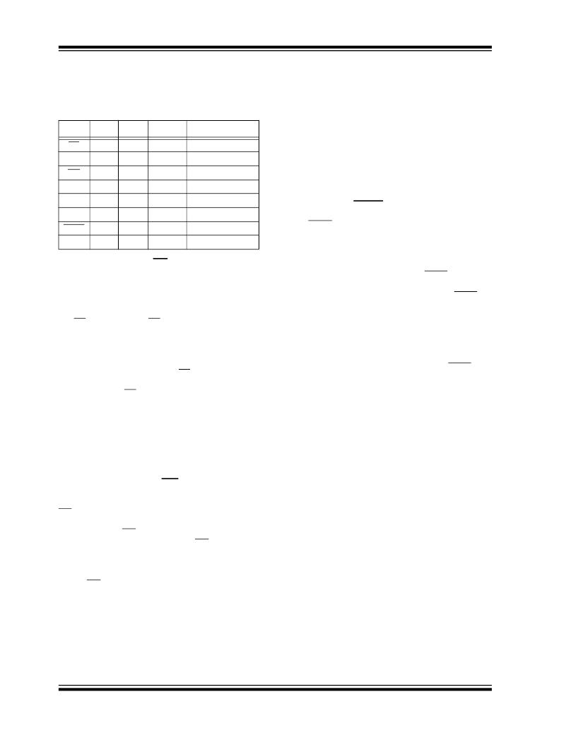
�TABLE� 2-1:�
�PIN� FUNCTION� TABLE�
�latched� on� the� rising� edge� of� the� serial� clock.�
�Name�
�PDIP�
�SOIC�
�TSSOP�
�Description�
�2.5�
�Serial� Clock� (SCK)�
�CS�
�SO�
�WP�
�V� SS�
�1�
�2�
�3�
�4�
�1�
�2�
�3�
�4�
�3�
�4�
�5�
�6�
�Chip� Select� Input�
�Serial� Data� Output�
�Write-Protect� Pin�
�Ground�
�The� SCK� is� used� to� synchronize� the� communication�
�between� a� master� and� the� 25XX040.� Instructions,�
�addresses� or� data� present� on� the� SI� pin� are� latched� on�
�the� rising� edge� of� the� clock� input,� while� data� on� the� SO�
�pin� is� updated� after� the� falling� edge� of� the� clock� input.�
�SI�
�SCK�
�5�
�6�
�5�
�6�
�7�
�8�
�Serial� Data� Input�
�Serial� Clock� Input�
�2.6�
�Hold� (HOLD)�
�HOLD�
�V� CC�
�7�
�8�
�7�
�8�
�1�
�2�
�Hold� Input�
�Supply� Voltage�
�The� HOLD� pin� is� used� to� suspend� transmission� to� the�
�25XX040� while� in� the� middle� of� a� serial� sequence�
�without� having� to� retransmit� the� entire� sequence� again�
�at� a� later� time.� It� must� be� held� high� any� time� this� func-�
�2.1�
�Chip� Select� (CS)�
�tion� is� not� being� used.� Once� the� device� is� selected� and�
�A� low� level� on� this� pin� selects� the� device.� A� high� level�
�deselects� the� device� and� forces� it� into� Standby� mode.�
�However,� a� programming� cycle� which� is� already�
�initiated� or� in� progress� will� be� completed,� regardless� of�
�the� CS� input� signal.� If� CS� is� brought� high� during� a�
�program� cycle,� the� device� will� go� in� Standby� mode� as�
�soon� as� the� programming� cycle� is� complete.� When� the�
�device� is� deselected,� SO� goes� into� the� high-impedance�
�state,� allowing� multiple� parts� to� share� the� same� SPI�
�bus.� A� low-to-high� transition� on� CS� after� a� valid� write�
�sequence� initiates� an� internal� write� cycle.� After� power-�
�up,� a� low� level� on� CS� is� required� prior� to� any� sequence�
�being� initiated.�
�a� serial� sequence� is� underway,� the� HOLD� pin� may� be�
�pulled� low� to� pause� further� serial� communication�
�without� resetting� the� serial� sequence.� The� HOLD� pin�
�must� be� brought� low� while� SCK� is� low,� otherwise� the�
�HOLD� function� will� not� be� invoked� until� the� next� SCK�
�high-to-low� transition.� The� 25XX040� must� remain�
�selected� during� this� sequence.� The� SI,� SCK� and� SO�
�pins� are� in� a� high-impedance� state� during� the� time� the�
�part� is� paused� and� transitions� on� these� pins� will� be�
�ignored.� To� resume� serial� communication,� HOLD� must�
�be� brought� high� while� the� SCK� pin� is� low,� otherwise�
�serial� communication� will� not� resume.� Lowering� the�
�HOLD� line� at� any� time� will� tri-state� the� SO� line.�
�2.2�
�Serial� Output� (SO)�
�The� SO� pin� is� used� to� transfer� data� out� of� the� 25XX040.�
�During� a� read� cycle,� data� is� shifted� out� on� this� pin� after�
�the� falling� edge� of� the� serial� clock.�
�2.3�
�Write-Protect� (WP)�
�Thi� s� pin� is� a� hardware� write-protect� input� pin.� When�
�WP� is� low,� all� writes� to� the� array� or� STATUS� register�
�are� disabled,� but� any� other� operation� functions�
�normally.� When� WP� is� high,� all� functions,� including�
�nonvolatile� writes� operate� normally.� WP� going� low� at�
�any� time� will� reset� the� write� enable� latch� and� inhibit�
�programming,� except� when� an� internal� write� has�
�already� begun.� If� an� internal� write� cycle� has� already�
�begun,� WP� going� low� will� have� no� effect� on� the� write.�
�See� Table� 3-3� for� Write-Protect� Functionality� Matrix.�
�DS21204E-page� 6�
�?� 2006� Microchip� Technology� Inc.�
�相关PDF资料 |
PDF描述 |
|---|---|
| 25AA080A-I/SN | IC EEPROM 8KBIT 10MHZ 8SOIC |
| 25LC080A-I/SN | IC EEPROM 8KBIT 10MHZ 8SOIC |
| 25LC020A-I/SN | IC EEPROM 2KBIT 10MHZ 8SOIC |
| M1A3PE1500-FGG676I | IC FPGA 1KB FLASH 1.5M 676-FBGA |
| 93LC76B-I/SN | IC EEPROM 8KBIT 2MHZ 8SOIC |
相关代理商/技术参数 |
参数描述 |
|---|---|
| 25C040-ISN | 制造商:未知厂家 制造商全称:未知厂家 功能描述:SPI Serial EEPROM |
| 25C040N | 制造商:未知厂家 制造商全称:未知厂家 功能描述:EEPROM |
| 25C040-P | 制造商:未知厂家 制造商全称:未知厂家 功能描述:SPI Serial EEPROM |
| 25C040-SN | 制造商:未知厂家 制造商全称:未知厂家 功能描述:SPI Serial EEPROM |
| 25C040ST | 制造商:未知厂家 制造商全称:未知厂家 功能描述:EEPROM |
发布紧急采购,3分钟左右您将得到回复。