- 您现在的位置:买卖IC网 > PDF目录33503 > 2SK3799 8 A, 900 V, 1.3 ohm, N-CHANNEL, Si, POWER, MOSFET PDF资料下载
参数资料
| 型号: | 2SK3799 |
| 元件分类: | JFETs |
| 英文描述: | 8 A, 900 V, 1.3 ohm, N-CHANNEL, Si, POWER, MOSFET |
| 封装: | LEAD FREE, 2-10U1B, SC-67, 3 PIN |
| 文件页数: | 2/6页 |
| 文件大小: | 190K |
| 代理商: | 2SK3799 |
2SK3799
2010-01-29
2
Lot No.
Note 4
K3799
Part No. (or abbreviation code)
Electrical Characteristics (Ta = 25°C)
Characteristic
Symbol
Test Condition
Min
Typ.
Max
Unit
Gate leakage current
IGSS
VGS = ±30 V, VDS = 0 V
—
±10
μA
Gate-source breakdown voltage
V (BR) GSS
IG = ±10 μA, VDS = 0 V
±30
—
V
Drain cut-off current
IDSS
VDS = 720 V, VGS = 0 V
—
100
μA
Drain-source breakdown voltage
V (BR) DSS
ID = 10 mA, VGS = 0 V
900
—
V
Gate threshold voltage
Vth
VDS = 10 V, ID = 1 mA
2.0
—
4.0
V
Drain-source ON-resistance
RDS (ON)
VGS = 10 V, ID = 4 A
—
1.0
1.3
Ω
Forward transfer admittance
|Yfs|
VDS = 15 V, ID = 4 A
3.5
6.0
—
S
Input capacitance
Ciss
—
2200
—
Reverse transfer capacitance
Crss
—
45
—
Output capacitance
Coss
VDS = 25 V, VGS = 0 V, f = 1 MHz
—
190
—
pF
Rise time
tr
—
25
—
Turn-on time
ton
—
65
—
Fall time
tf
—
20
—
Switching time
Turn-off time
toff
Duty ≤ 1%, tw = 10 μs
—
120
—
ns
Total gate charge (Gate-source
plus gate-drain)
Qg
—
60
—
Gate-source charge
Qgs
—
34
—
Gate-drain (“miller”) charge
Qgd
VDD ≈ 400 V, VGS = 10 V, ID = 8 A
—
26
—
nC
Source-Drain Ratings and Characteristics (Ta = 25°C)
Characteristic
Symbol
Test Condition
Min
Typ.
Max
Unit
Continuous drain reverse current
(Note 1)
IDR
—
8
A
Pulse drain reverse current
(Note 1)
IDRP
—
24
A
Forward voltage (diode)
VDSF
IDR = 8 A, VGS = 0 V
—
1.7
V
Reverse recovery time
trr
—
1700
—
ns
Reverse recovery charge
Qrr
IDR = 8 A, VGS = 0 V
dlDR / dt = 100 A / μs
—
23
—
μC
Marking
0 V
10 V
VGS
R
L=
100
Ω
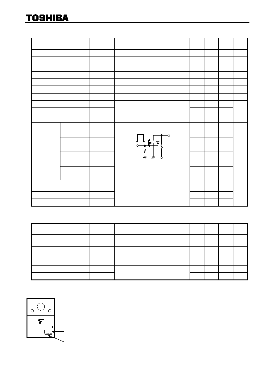
VDD ≈ 400 V
ID = 4 A Output
4.7
Ω
Note 4: A line under a Lot No. identifies the indication of product
Labels.
Not underlined: [[Pb]]/INCLUDES > MCV
Underlined: [[G]]/RoHS COMPATIBLE or [[G]]/RoHS [[Pb]]
Please contact your TOSHIBA sales representative for details as to
environmental matters such as the RoHS compatibility of Product.
The RoHS is the Directive 2002/95/EC of the European Parliament
and of the Council of 27 January 2003 on the restriction of the use of
certain hazardous substances in electrical and electronic equipment.
相关PDF资料 |
PDF描述 |
|---|---|
| 2SK381-11-B | N-CHANNEL, Si, SMALL SIGNAL, JFET |
| 2SK381-11-C | N-CHANNEL, Si, SMALL SIGNAL, JFET |
| 2SK381-11-A | N-CHANNEL, Si, SMALL SIGNAL, JFET |
| 2SK381-T11-C | N-CHANNEL, Si, SMALL SIGNAL, JFET |
| 2SK381-11-E | N-CHANNEL, Si, SMALL SIGNAL, JFET |
相关代理商/技术参数 |
参数描述 |
|---|---|
| 2SK3799(Q) | 制造商:Toshiba America Electronic Components 功能描述:TRANS MOSFET N-CH 900V 8A 3PIN SC-67 - Rail/Tube 制造商:Toshiba 功能描述:Nch 900V 8A 1.3@10V TO220SIS Bulk 制造商:Toshiba America Electronic Components 功能描述:Transistor,MOSFET |
| 2SK3799(Q,M) | 制造商:Toshiba America Electronic Components 功能描述:TRANS MOSFET N-CH - Rail/Tube 制造商:Toshiba America Electronic Components 功能描述:MOSFET N-CH 900V 8A TO220SIS 制造商:Toshiba 功能描述:TRANSISTOR |
| 2SK3799(STA4,Q) | 制造商:Toshiba America Electronic Components 功能描述: |
| 2SK3799(STA4,Q,M) | 制造商:Toshiba America Electronic Components 功能描述:MOSFET |
| 2SK3800 | 功能描述:MOSFET N-CH 40V TO-220S 制造商:sanken 系列:- 包装:带卷(TR) 零件状态:新产品 FET 类型:MOSFET N 通道,金属氧化物 FET 功能:标准 漏源极电压(Vdss):40V 电流 - 连续漏极(Id)(25°C 时):70A(Ta) 不同?Id,Vgs 时的?Rds On(最大值):6 毫欧 @ 35A,10V 不同 Id 时的 Vgs(th)(最大值):4V @ 1mA 不同 Vgs 时的栅极电荷(Qg):- 不同 Vds 时的输入电容(Ciss):5100pF @ 10V 功率 - 最大值:80W 工作温度:150°C(TJ) 安装类型:表面贴装 封装/外壳:TO-263-3,D2Pak(2 引线+接片),TO-263AB 供应商器件封装:TO-220S 标准包装:1,000 |
发布紧急采购,3分钟左右您将得到回复。