- 您现在的位置:买卖IC网 > PDF目录33797 > 45AZ (Intersil Corporation) 5V or 12V Single Synchronous Buck Pulse-Width Modulation (PWM) Controller PDF资料下载
参数资料
| 型号: | 45AZ |
| 厂商: | Intersil Corporation |
| 英文描述: | 5V or 12V Single Synchronous Buck Pulse-Width Modulation (PWM) Controller |
| 中文描述: | 单5V或12V同步降压脉宽调制(PWM)控制器 |
| 文件页数: | 3/16页 |
| 文件大小: | 302K |
| 代理商: | 45AZ |
www.DataSheet4U.com
11
FN6305.3
November 15, 2006
The modulator transfer function is the small-signal transfer
function of VOUT/VCOMP. This function is dominated by a DC
gain, given by dMAXVIN/VOSC, and shaped by the output
filter, with a double pole break frequency at FLC and a zero at
FCE. For the purpose of this analysis, L and D represent the
channel inductance and its DCR, while C and E represent the
total output capacitance and its equivalent series resistance.
The compensation network consists of the error amplifier
(internal to the ISL6545) and the external R1-R3, C1-C3
components. The goal of the compensation network is to
provide a closed loop transfer function with high 0dB crossing
frequency (F0; typically 0.1 to 0.3 of FSW) and adequate phase
margin (better than 45°). Phase margin is the difference
between the closed loop phase at F0dB and 180°. The
equations that follow relate the compensation network’s poles,
zeros and gain to the components (R1, R2, R3, C1, C2, and
C3) in Figure 9. Use the following guidelines for locating the
poles and zeros of the compensation network:
4. Select a value for R1 (1k
Ω to 5kΩ, typically). Calculate
value for R2 for desired converter bandwidth (F0). If
setting the output voltage via an offset resistor connected
to the FB pin, Ro in Figure 9, the design procedure can
be followed as presented.
5. Calculate C1 such that FZ1 is placed at a fraction of the FLC,
at 0.1 to 0.75 of FLC (to adjust, change the 0.5 factor to
desired number). The higher the quality factor of the output
filter and/or the higher the ratio FCE/FLC, the lower the FZ1
frequency (to maximize phase boost at FLC).
6. Calculate C2 such that FP1 is placed at FCE.
7. Calculate R3 such that FZ2 is placed at FLC. Calculate C3
such that FP2 is placed below FSW (typically, 0.5 to 1.0
times FSW). FSW represents the switching frequency.
Change the numerical factor to reflect desired placement
of this pole. Placement of FP2 lower in frequency helps
reduce the gain of the compensation network at high
frequency, in turn reducing the HF ripple component at
the COMP pin and minimizing resultant duty cycle jitter.
It is recommended a mathematical model is used to plot the
loop response. Check the loop gain against the error
amplifier’s open-loop gain. Verify phase margin results and
adjust as necessary. The following equations describe the
frequency response of the modulator (GMOD), feedback
compensation (GFB) and closed-loop response (GCL):
COMPENSATION BREAK FREQUENCY EQUATIONS
Figure 10 shows an asymptotic plot of the DC/DC converter’s
gain vs. frequency. The actual Modulator Gain has a high gain
peak dependent on the quality factor (Q) of the output filter,
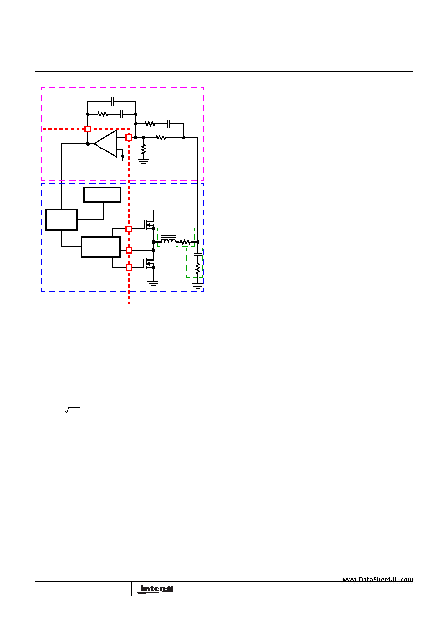
FIGURE 9. VOLTAGE-MODE BUCK CONVERTER
COMPENSATION DESIGN
-
+
E/A
VREF
COMP
C1
R2
R1
FB
C2
R3
C3
L
C
VIN
PWM
CIRCUIT
HALF-BRIDGE
DRIVE
OSCILLATOR
E
EXTERNAL CIRCUIT
ISL6545
VOUT
VOSC
D
UGATE
LGATE
Ro
PHASE
F
LC
1
2
π
LC
---------------------------
=
F
CE
1
2
π CE
------------------------
=
R2
V
OSC R1 F0
d
MAX VIN FLC
---------------------------------------------
=
C1
1
2
π R2 0.5 F
LC
------------------------------------------------
=
C2
C1
2
π R2 C1 F
CE
1
–
---------------------------------------------------------
=
R3
R1
F
SW
F
LC
------------
1
–
----------------------
=
C3
1
2
π R3 0.7 F
SW
-------------------------------------------------
=
G
MOD f
()
d
MAX VIN
V
OSC
------------------------------
1s f
() EC
+
1s f
() ED
+
() C
s
2
f
() LC
++
----------------------------------------------------------------------------------------
=
G
FB f
()
1s f
() R2 C1
+
sf
() R1 C1 C2
+
()
------------------------------------------------------
=
1s f
() R1 R3
+
() C3
+
1s f
() R3 C3
+
() 1s f
() R2
C1 C2
C1
C2
+
----------------------
+
-----------------------------------------------------------------------------------------------------------------------------
G
CL f
()
G
MOD f
() G
FB f
()
=
where s f
()
,
2
π fj
=
F
Z1
1
2
π R2 C1
--------------------------------
=
F
Z2
1
2
π R1 R3
+
() C3
---------------------------------------------------
=
F
P1
1
2
π R2 C1 C2
C1
C2
+
----------------------
-----------------------------------------------
=
F
P2
1
2
π R3 C3
--------------------------------
=
ISL6545, ISL6545A
相关PDF资料 |
PDF描述 |
|---|---|
| 45CIQ100 | 45Amp Schottky Rectifier(45A 肖特基整流器) |
| 45CIQ | SCHOTTKY RECTIFIER |
| 45DB011B | 1-Megabit 2.7-volt Only Serial DataFlash |
| 45DB041B | 4-megabit 2.5-volt Only or 2.7-volt Only DataFlash |
| 45DB081B | AT-45DB081B DATA FLASH RELIABILITY DATA |
相关代理商/技术参数 |
参数描述 |
|---|---|
| 45B009 | 制造商:CSYS 功能描述: |
| 45BKB | 制造商:Thomas & Betts 功能描述:BLACKBURN POWDER |
| 45C | 制造商:American Beauty Tools 功能描述:Soldering Iron Tip, Chisel Style, Used in Model 3178 制造商:American Beauty Tools 功能描述:Chisel Style Soldering Tip |
| 45CA20AJ | 制造商: 功能描述: 制造商:undefined 功能描述: |
| 45-CBSA-0.5X0.5X0.4 | 功能描述:45 SERIES CBS SHIELD ASSEMBLY 制造商:leader tech inc. 系列:* 零件状态:在售 标准包装:27 |
发布紧急采购,3分钟左右您将得到回复。