- 您现在的位置:买卖IC网 > PDF目录67337 > 5962-9451801MLX (ANALOG DEVICES INC) DUAL, PARALLEL, WORD INPUT LOADING, 3 us SETTLING TIME, 12-BIT DAC, CDIP24 PDF资料下载
参数资料
| 型号: | 5962-9451801MLX |
| 厂商: | ANALOG DEVICES INC |
| 元件分类: | DAC |
| 英文描述: | DUAL, PARALLEL, WORD INPUT LOADING, 3 us SETTLING TIME, 12-BIT DAC, CDIP24 |
| 封装: | 0.300 INCH, GLASS SEALED, CERDIP-24 |
| 文件页数: | 12/13页 |
| 文件大小: | 193K |
| 代理商: | 5962-9451801MLX |
AD7837/AD7847
REV. C
–8–
VALID
DATA
t6
t3
t8
WR
DATA
ADDRESS DATA
t7
t1
t2
t5
t4
CS
A0/A1
LDAC
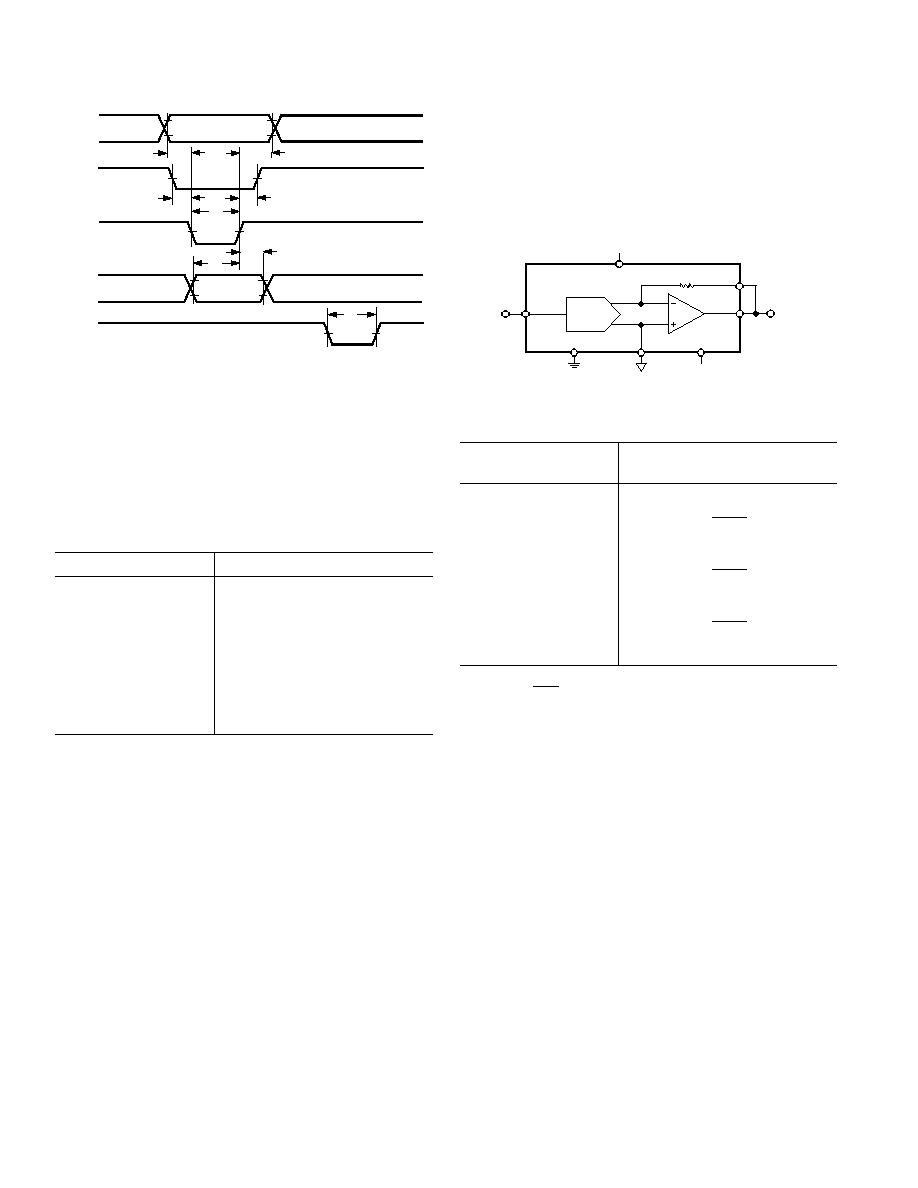
Figure 14. AD7837 Write Cycle Timing Diagram
CS, WR, A0 and A1 control the loading of data to the input
latches. The eight data inputs accept right-justified data. Data
can be loaded to the input latches in any sequence. Provided that
LDAC is held high, there is no analog output change as a result
of loading data to the input latches. Address lines A0 and A1
determine which latch data is loaded to when
CS and WR are low.
The control logic truth table for the part is shown in Table II.
Table II. AD7837 Truth Table
CS WR A1 A0 LDAC Function
1
X
1
No Data Transfer
X
1
X
1
No Data Transfer
0
1
DAC A LS Input Latch Transparent
0
1
DAC A MS Input Latch Transparent
0
1
0
1
DAC B LS Input Latch Transparent
0
1
DAC B MS Input Latch Transparent
1
X
0
DAC A and DAC B DAC Latches
Updated Simultaneously from the
Respective Input Latches
X = Don’t Care.
The
LDAC input controls the transfer of 12-bit data from the
input latches to the DAC latches. When
LDAC is taken low, both
DAC latches, and hence both analog outputs, are updated at
the same time. The data in the DAC latches is held on the rising
edge of
LDAC. The LDAC input is asynchronous and indepen-
dent of
WR. This is useful in many applications especially in the
simultaneous updating of multiple AD7837s. However, care must
be taken while exercising
LDAC during a write cycle. If an LDAC
operation overlaps a
CS and WR operation, there is a possibility
of invalid data being latched to the output. To avoid this,
LDAC
must remain low after
CS or WR return high for a period equal
to or greater than t8, the minimum LDAC pulsewidth.
UNIPOLAR BINARY OPERATION
Figure 15 shows DAC A on the AD7837/AD7847 connected
for unipolar binary operation. Similar connections apply for
DAC B. When VIN is an ac signal, the circuit performs 2-quad-
rant multiplication. The code table for this circuit is shown in
Table III. Note that on the AD7847 the feedback resistor RFB is
internally connected to VOUT.
DAC A
AGNDA
VOUTA
VREFA
VIN
DGND
VSS
RFBA
*
VSS
VDD
AD7837
AD7847
VOUT
*INTERNALLY
CONNECTED
ON AD7847
Figure 15. Unipolar Binary Operation
Table III. Unipolar Code Table
DAC Latch Contents
MSB
LSB
Analog Output, VOUT
1111 1111 1111
–VIN
×
4095
4096
1000 0000 0000
–VIN
×
2048
4096
= –1/ 2 V
IN
0000 0000 0001
–VIN
×
1
4096
0000 0000 0000
0 V
Note 1 LSB =
V
IN
4096
.
相关PDF资料 |
PDF描述 |
|---|---|
| 5962-9452702M2C | QUAD, SERIAL INPUT LOADING, 8-BIT DAC, CQCC20 |
| 5962-9452702MEA | QUAD, SERIAL INPUT LOADING, 8-BIT DAC, CDIP16 |
| 5962-9453001M2A | 2 A SWITCHING CONTROLLER, 230 kHz SWITCHING FREQ-MAX, CQCC20 |
| 5962-9453001MEA | 2 A SWITCHING CONTROLLER, 230 kHz SWITCHING FREQ-MAX, CDIP16 |
| 5962-9455501M3A | 3 A SWITCHING CONTROLLER, 2000 kHz SWITCHING FREQ-MAX, CQCC28 |
相关代理商/技术参数 |
参数描述 |
|---|---|
| 5962-9451802MLA | 功能描述:数模转换器- DAC DUAL 12-BIT DAC IC RoHS:否 制造商:Texas Instruments 转换器数量:1 DAC 输出端数量:1 转换速率:2 MSPs 分辨率:16 bit 接口类型:QSPI, SPI, Serial (3-Wire, Microwire) 稳定时间:1 us 最大工作温度:+ 85 C 安装风格:SMD/SMT 封装 / 箱体:SOIC-14 封装:Tube |
| 5962-9452101M2A | 制造商:Analog Devices 功能描述:OP Amp Quad GP 制造商:Analog Devices 功能描述:OP AMP QUAD GP 20V 20PIN LCC - Rail/Tube 制造商:Analog Devices Inc. 功能描述:QUAD PICO AMP 制造商:Analog Devices Inc. 功能描述:High Speed Operational Amplifiers QUAD PICO AMP |
| 5962-9452201MXA | 制造商:Cypress Semiconductor 功能描述: |
| 5962-9452201MXX | 制造商:Cypress Semiconductor 功能描述: 制造商:Rochester Electronics LLC 功能描述: |
| 5962-9452601Q2A | 制造商:Texas Instruments 功能描述:Comparator Dual |
发布紧急采购,3分钟左右您将得到回复。