- 您现在的位置:买卖IC网 > PDF目录67337 > 5962-9451801MLX (ANALOG DEVICES INC) DUAL, PARALLEL, WORD INPUT LOADING, 3 us SETTLING TIME, 12-BIT DAC, CDIP24 PDF资料下载
参数资料
| 型号: | 5962-9451801MLX |
| 厂商: | ANALOG DEVICES INC |
| 元件分类: | DAC |
| 英文描述: | DUAL, PARALLEL, WORD INPUT LOADING, 3 us SETTLING TIME, 12-BIT DAC, CDIP24 |
| 封装: | 0.300 INCH, GLASS SEALED, CERDIP-24 |
| 文件页数: | 13/13页 |
| 文件大小: | 193K |
| 代理商: | 5962-9451801MLX |
AD7837/AD7847
REV. C
–9–
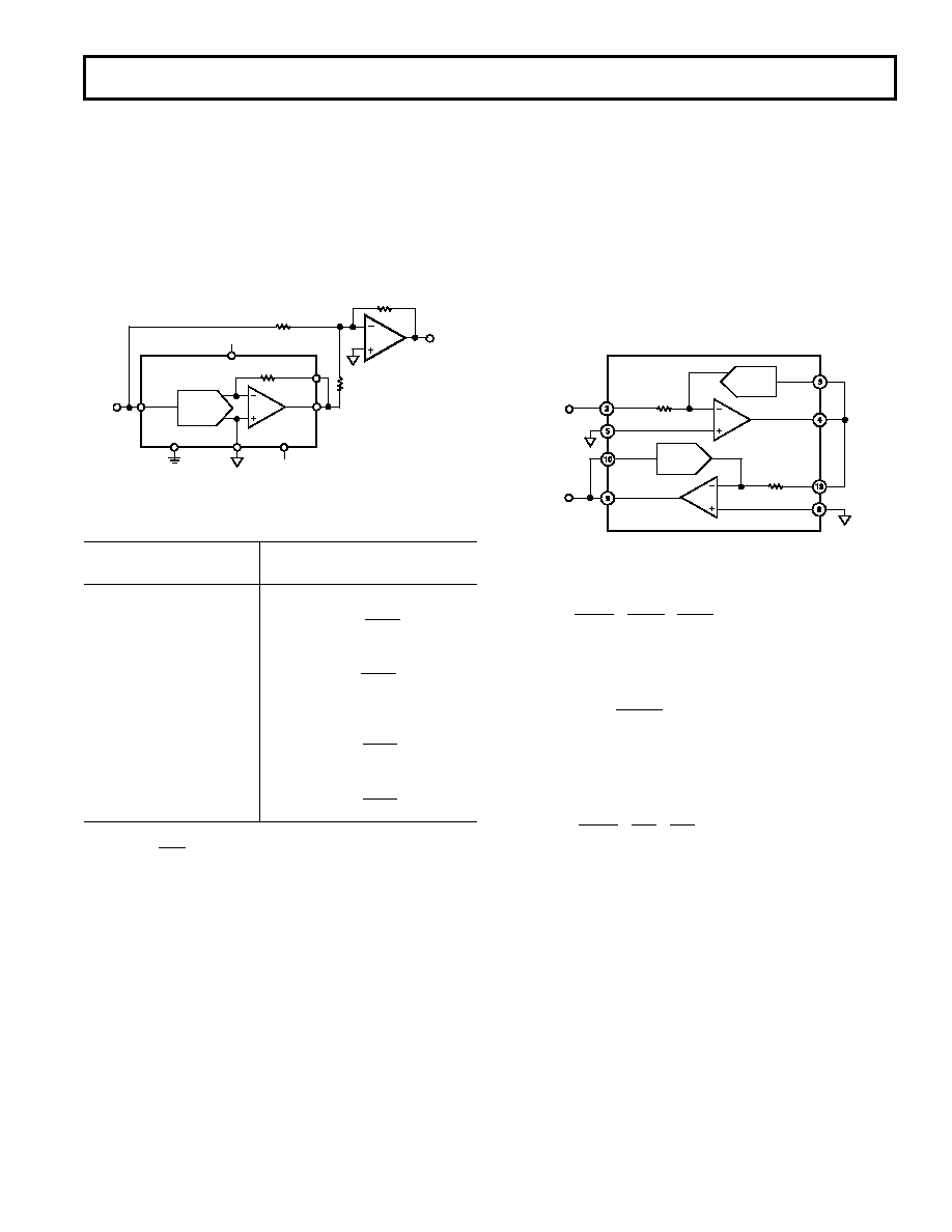
APPLICATIONS
PROGRAMMABLE GAIN AMPLIFIER (PGA)
The dual DAC/amplifier combination along with access to RFB
make the AD7837 ideal as a programmable gain amplifier. In this
application, the DAC functions as a programmable resistor in the
amplifier feedback loop. This type of configuration is shown
in Figure 17 and is suitable for ac gain control. The circuit con-
sists of two PGAs in series. Use of a dual configuration provides
greater accuracy over a wider dynamic range than a single PGA
solution. The overall system gain is the product of the individual
gain stages. The effective gains for each stage are controlled by
the DAC codes. As the code decreases, the effective DAC
resistance increases, and so the gain also increases.
DAC B
AGNDA
VOUTB
VREFB
VIN
RFBB
AD7837
VOUT
RFBA
AGNDB
DAC A
VOUTA
VREFA
Figure 17. Dual PGA Circuit
The transfer function is given by
VOUT
VIN
=
REQA
RFBA
×
REQB
RFBB
(1)
where REQA, REQB are the effective DAC resistances controlled
by the digital input code:
REQ
=
212 RIN
N
(2)
where RIN is the DAC input resistance and is equal to RFB and
N = DAC input code in decimal.
The transfer function in (1) thus simplifies to
VOUT
VIN
=
212
N A
×
212
NB
(3)
where NA = DAC A input code in decimal and NB = DAC B
input code in decimal.
NA, NB may be programmed between 1 and (2
12–1). The zero
code is not allowed as it results in an open loop amplifier
response. To minimize errors, the digital codes NA and NB
should be chosen to be equal to or as close as possible to each
other to achieve the required gain.
BIPOLAR OPERATION
(4-QUADRANT MULTIPLICATION)
Figure 16 shows the AD7837/AD7847 connected for bipolar
operation. The coding is offset binary as shown in Table IV.
When VIN is an ac signal, the circuit performs 4-quadrant multi-
plication. To maintain the gain error specifications, resistors R1,
R2 and R3 should be ratio matched to 0.01%. Note that on the
AD7847 the feedback resistor RFB is internally connected to
VOUT.
DAC A
AGNDA
VOUTA
VREFA
VIN
DGND
VSS
RFBA
*
VDD
AD7837
AD7847
*INTERNALLY
CONNECTED
ON AD7847
R3
10k
R1
20k
AD711
R2
20k
VOUT
VSS
Figure 16. Bipolar Offset Binary Operation
Table IV. Bipolar Code Table
DAC Latch Contents
MSB
LSB
Analog Output, VOUT
1111 1111 1111
+V
IN
×
2047
2048
1000 0000 0001
+V
IN
×
1
2048
1000 0000 0000
0 V
0111 1111 1111
–VIN
×
1
2048
0000 0000 0000
–VIN
×
2048
= –V
IN
Note 1 LSB =
V
IN
2048
.
相关PDF资料 |
PDF描述 |
|---|---|
| 5962-9452702M2C | QUAD, SERIAL INPUT LOADING, 8-BIT DAC, CQCC20 |
| 5962-9452702MEA | QUAD, SERIAL INPUT LOADING, 8-BIT DAC, CDIP16 |
| 5962-9453001M2A | 2 A SWITCHING CONTROLLER, 230 kHz SWITCHING FREQ-MAX, CQCC20 |
| 5962-9453001MEA | 2 A SWITCHING CONTROLLER, 230 kHz SWITCHING FREQ-MAX, CDIP16 |
| 5962-9455501M3A | 3 A SWITCHING CONTROLLER, 2000 kHz SWITCHING FREQ-MAX, CQCC28 |
相关代理商/技术参数 |
参数描述 |
|---|---|
| 5962-9451802MLA | 功能描述:数模转换器- DAC DUAL 12-BIT DAC IC RoHS:否 制造商:Texas Instruments 转换器数量:1 DAC 输出端数量:1 转换速率:2 MSPs 分辨率:16 bit 接口类型:QSPI, SPI, Serial (3-Wire, Microwire) 稳定时间:1 us 最大工作温度:+ 85 C 安装风格:SMD/SMT 封装 / 箱体:SOIC-14 封装:Tube |
| 5962-9452101M2A | 制造商:Analog Devices 功能描述:OP Amp Quad GP 制造商:Analog Devices 功能描述:OP AMP QUAD GP 20V 20PIN LCC - Rail/Tube 制造商:Analog Devices Inc. 功能描述:QUAD PICO AMP 制造商:Analog Devices Inc. 功能描述:High Speed Operational Amplifiers QUAD PICO AMP |
| 5962-9452201MXA | 制造商:Cypress Semiconductor 功能描述: |
| 5962-9452201MXX | 制造商:Cypress Semiconductor 功能描述: 制造商:Rochester Electronics LLC 功能描述: |
| 5962-9452601Q2A | 制造商:Texas Instruments 功能描述:Comparator Dual |
发布紧急采购,3分钟左右您将得到回复。