- 您现在的位置:买卖IC网 > PDF目录67337 > 5962-9451801MLX (ANALOG DEVICES INC) DUAL, PARALLEL, WORD INPUT LOADING, 3 us SETTLING TIME, 12-BIT DAC, CDIP24 PDF资料下载
参数资料
| 型号: | 5962-9451801MLX |
| 厂商: | ANALOG DEVICES INC |
| 元件分类: | DAC |
| 英文描述: | DUAL, PARALLEL, WORD INPUT LOADING, 3 us SETTLING TIME, 12-BIT DAC, CDIP24 |
| 封装: | 0.300 INCH, GLASS SEALED, CERDIP-24 |
| 文件页数: | 3/13页 |
| 文件大小: | 193K |
| 代理商: | 5962-9451801MLX |
AD7837/AD7847
REV. C
–11–
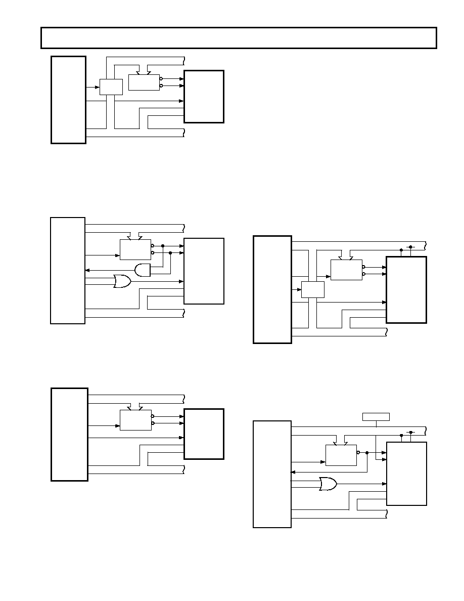
MICROPROCESSOR INTERFACING–AD7837
Figures 23 to 25 show the AD7837 configured for interfacing to
microprocessors with 8-bit data bus systems. In all cases, data is
right-justified and the AD7837 is memory-mapped with the two
lowest address lines of the microprocessor address bus driving
the A0 and A1 inputs of the AD7837. Five separate memory
addresses are required, one for the each MS latch and one for
each LS latch and one for the common
LDAC input. Data is
written to the respective input latch in two write operations.
Either high byte or low byte data can be written first to the
input latch. A write to the AD7837
LDAC address transfers the
data from the input latches to the respective DAC latches and
updates both analog outputs. Alternatively, the
LDAC input
can be asynchronous and can be common to several AD7837s
for simultaneous updating of a number of voltage channels.
AD7837–8051/8088 Interface
Figure 23 shows the connection diagram for interfacing the
AD7837 to both the 8051 and the 8088. On the 8051, the
signal
PSEN is used to enable the address decoder while DEN
is used on the 8088.
ADDRESS
DECODE
CS
LDAC
WR
DB7
DB0
ALE
AD7
AD0
8051/8088
AD7837*
ADDRESS BUS
ADDRESS/DATA BUS
OCTAL
LATCH
WR
*ADDITIONAL PINS OMITTED FOR CLARITY
A0 A1
EN
A15
A8
PSEN OR DEN
Figure 23. AD7837 to 8051/8088 Interface
AD7837–MC68008 Interface
An interface between the AD7837 and the MC68008 is shown
in Figure 24. In the diagram shown, the
LDAC signal is derived
from an asynchronous timer but this can be derived from the
address decoder as in the previous interface diagram.
WR
R/
W
DS
DTACK
ADDRESS
DECODE
CS
LDAC
DB7
DB0
D7
D0
AD7837*
ADDRESS BUS
DATA BUS
*ADDITIONAL PINS OMITTED FOR CLARITY
A0 A1
EN
A19
A0
AS
TIMER
MC68008
Figure 24. AD7837 to 68008 Interface
ADDRESS
DECODE
CSA
CSB
WR
DB11
DB0
ALE
AD15
AD0
8086
AD7847*
ADDRESS BUS
ADDRESS/DATA BUS
16 BIT
LATCH
WR
*ADDITIONAL PINS OMITTED FOR CLARITY
Figure 20. AD7847 to 8086 Interface
AD7847–MC68000 Interface
Figure 21 shows an interface between the AD7847 and the
MC68000. Once again a single MOVE instruction loads the
12-bit word into the selected DAC latch.
CSA and CSB are
AND-gated to provide a
DTACK signal when either DAC
latch is selected.
ADDRESS
DECODE
CSA
CSB
WR
DB11
DB0
A23
A1
MC68000
AD7847*
ADDRESS BUS
DATA BUS
AS
*ADDITIONAL PINS OMITTED FOR CLARITY
EN
R/
W
D15
D0
LDS
DTACK
Figure 21. AD7847 to MC68000 Interface
AD7847–TMS320C10 Interface
Figure 22 shows an interface between the AD7847 and the
TMS320C10 DSP processor. A single OUT instruction loads
the 12-bit word into the selected DAC latch.
ADDRESS
DECODE
CSA
CSB
WR
DB11
DB0
A11
A0
TMS320C10
AD7847*
ADDRESS BUS
DATA BUS
WE
*ADDITIONAL PINS OMITTED FOR CLARITY
EN
D15
D0
MEN
Figure 22. AD7847 to TMS320C10 Interface
相关PDF资料 |
PDF描述 |
|---|---|
| 5962-9452702M2C | QUAD, SERIAL INPUT LOADING, 8-BIT DAC, CQCC20 |
| 5962-9452702MEA | QUAD, SERIAL INPUT LOADING, 8-BIT DAC, CDIP16 |
| 5962-9453001M2A | 2 A SWITCHING CONTROLLER, 230 kHz SWITCHING FREQ-MAX, CQCC20 |
| 5962-9453001MEA | 2 A SWITCHING CONTROLLER, 230 kHz SWITCHING FREQ-MAX, CDIP16 |
| 5962-9455501M3A | 3 A SWITCHING CONTROLLER, 2000 kHz SWITCHING FREQ-MAX, CQCC28 |
相关代理商/技术参数 |
参数描述 |
|---|---|
| 5962-9451802MLA | 功能描述:数模转换器- DAC DUAL 12-BIT DAC IC RoHS:否 制造商:Texas Instruments 转换器数量:1 DAC 输出端数量:1 转换速率:2 MSPs 分辨率:16 bit 接口类型:QSPI, SPI, Serial (3-Wire, Microwire) 稳定时间:1 us 最大工作温度:+ 85 C 安装风格:SMD/SMT 封装 / 箱体:SOIC-14 封装:Tube |
| 5962-9452101M2A | 制造商:Analog Devices 功能描述:OP Amp Quad GP 制造商:Analog Devices 功能描述:OP AMP QUAD GP 20V 20PIN LCC - Rail/Tube 制造商:Analog Devices Inc. 功能描述:QUAD PICO AMP 制造商:Analog Devices Inc. 功能描述:High Speed Operational Amplifiers QUAD PICO AMP |
| 5962-9452201MXA | 制造商:Cypress Semiconductor 功能描述: |
| 5962-9452201MXX | 制造商:Cypress Semiconductor 功能描述: 制造商:Rochester Electronics LLC 功能描述: |
| 5962-9452601Q2A | 制造商:Texas Instruments 功能描述:Comparator Dual |
发布紧急采购,3分钟左右您将得到回复。